Package structure and package process of light emitting diode

a technology of light-emitting diodes and packaging structures, which is applied in the manufacture of semiconductor/solid-state devices, electrical equipment, semiconductor devices, etc., can solve the problems of high fabrication cost of phosphor coating layers, and achieve the effect of low fabrication cost and high illumination efficiency

Active Publication Date: 2012-12-11
ADVANCED SEMICON ENG INC
View PDF6 Cites 2 Cited by
  • Summary
  • Abstract
  • Description
  • Claims
  • Application Information

AI Technical Summary

Benefits of technology

[0007]Accordingly, the present invention is directed to an LED package structure capable of providing uniform light output and having high illuminating efficiency and low fabrication cost.

Problems solved by technology

Nonetheless, the fabrication cost of the phosphor coating layer goes high due to performing a wafer level coating process.

Method used


Image

  • Package structure and package process of light emitting diode
  • Package structure and package process of light emitting diode
  • Package structure and package process of light emitting diode

Examples


Embodiment Construction

[0017]Reference will now be made in detail to the present preferred embodiments of the invention, examples of which are illustrated in the accompanying drawings. Wherever possible, the same reference numbers are used in the drawings and the description to refer to the same or like parts.

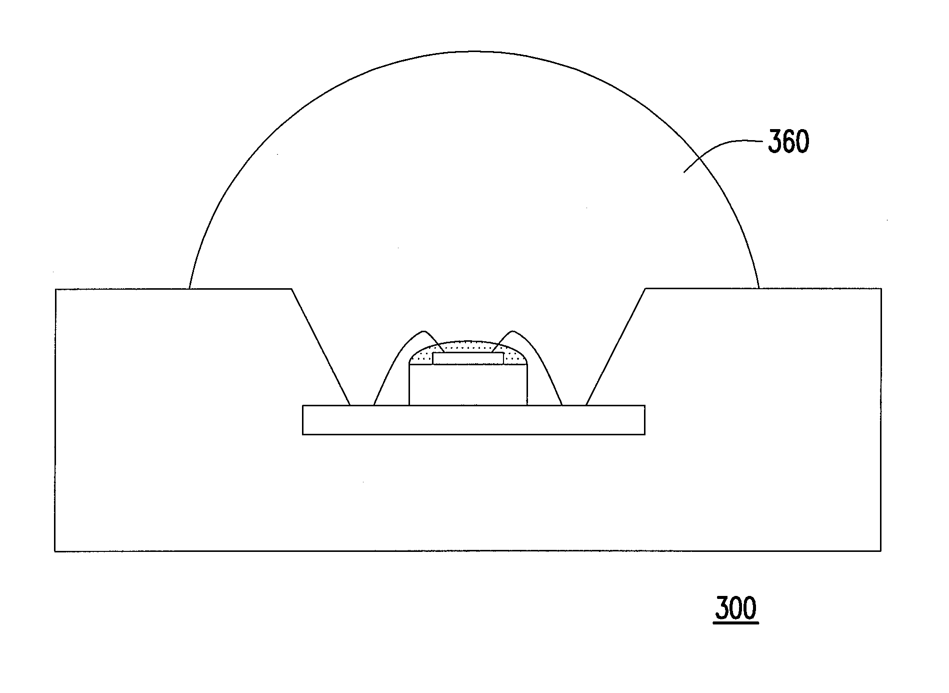
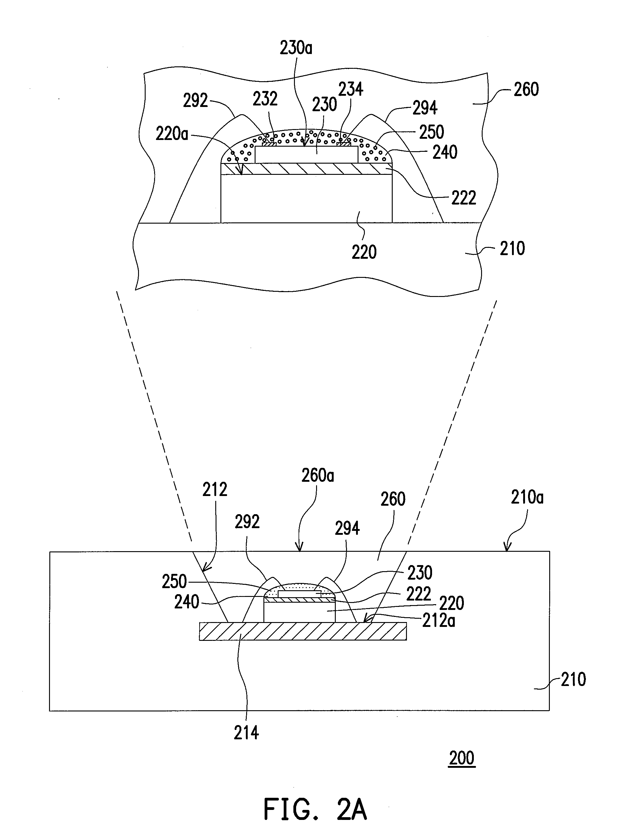
[0018]FIGS. 2A and 2B are cross-sectional views showing LED package structures according to an embodiment of the present invention. Referring to FIGS. 2A and 2B, the LED package structure 200 comprises a carrier 210, a spacer 220, at least one LED chip 230, a junction coating 240, a plurality of phosphor particles250, and an encapsulant 260. In the present embodiment, the carrier 210 is, for example, a pre-molded metal leadframe having a cavity 212. A bonding pad 214 is exposed by the bottom surface 212a of the cavity 212. In other embodiments, the carrier 210 can further be, for example, a metal leadframe or a ceramic substrate, while the type of the carrier 210 of the present invention is not limit...


PUM


Abstract

A light emitted diode (LED) package structure and an LED package process are provided. The LED package structure comprises a carrier, a spacer, at least one LED chip, a junction coating, a plurality of phosphor particles, and an encapsulant. The spacer is disposed on the carrier and provided with a reflective layer covering a top surface of the spacer. The LED chip is disposed on the reflective layer and electrically connected to the carrier. The junction coating is disposed over the spacer and covers the LED chip. The phosphor particles are distributed within the junction coating. The encapsulant is disposed on the carrier and encapsulates the LED chip, the spacer and the junction coating. Uniform light output and high illuminating efficiency can be obtained by the phosphor particles uniformly distributed in the junction coating. The junction coating is formed by package level dispensing process to reduce the fabrication cost.

Description

BACKGROUND OF THE INVENTION[0001]1. Field of the Invention[0002]The present invention generally relates to a structure and a fabricating method of a light source. More particularly, the present invention relates to a package structure and a package process of light emitting diode (LED).[0003]2. Description of Related Art[0004]Light emitting diodes (LEDs) have replaced fluorescent lamps and incandescent lamps in some fields, for example, lamps of scanners requiring for quick response, lamps of projection apparatus, backlight sources or front light sources of liquid crystal displays (LCDs), illumination for dashboards of automobiles, traffic lights, common illumination devices, etc. Compared with conventional lamps, the LEDs have absolute advantages, for example, small volume, long lifespan, low driving voltage / current, non-fragile, mercury free (no pollution), and good luminous efficiency (power saving).[0005]FIG. 1 is a cross-sectional view showing a conventional white LED package s...

Claims


Application Information

Patent Timeline
Patent Type & Authority Patents(United States)
IPC IPC(8): H01L33/00
CPCH01L33/60H01L33/501H01L33/502H01L33/54H01L2933/0091H01L2224/8592H01L2224/48091H01L2924/00014
Inventor JEONG, HYUNSOOLEE, SEONGOOPARK, RYUNGSHIKLEE, HYUNIL
Owner ADVANCED SEMICON ENG INC
Why Eureka
Try Eureka