Liquid crystal display device and electronic device

a technology of liquid crystal display and electronic device, which is applied in the direction of semiconductor devices, instruments, optics, etc., can solve the problems of reducing the aperture ratio of a pixel, increasing the size of the transistor, and low current drive capability of a transistor using amorphous semiconductors, so as to achieve improved aperture ratio and high-quality electronic devices

Active Publication Date: 2012-12-11
SEMICON ENERGY LAB CO LTD
View PDF77 Cites 19 Cited by
  • Summary
  • Abstract
  • Description
  • Claims
  • Application Information

AI Technical Summary

Benefits of technology

[0009]In a liquid crystal display device, high current drive capability and low leakage current characteristics are needed for a transistor of a pixel portion (hereinafter, also referred to as a “pixel transistor”). High current drive capability is needed in order to perform charging or discharging of a storage capacitor in a rapid manner. Low leakage current characteristics are needed in order to save electric charges stored in a storage capacitor.
[0010]When the amorphous semiconductor is used as a pixel transistor, there is an advantage that manufacturing cost is low. On the other hand, since the amorphous semiconductor has low carrier mobility, current drive capability of a transistor using the amorphous semiconductor is also low. Improvement of current drive capability is possible by increase of the channel width of a transistor. However, the size of the transistor increases in this case, whereby a problem of decreasing the aperture ratio of a pixel is caused.
[0015]In view of such problems, it is an object of the present invention to provide a liquid crystal display device and an electronic device with improved aperture ratio.
[0016]In the present invention, a transistor is manufactured using a stacked structure of semiconductor having a microcrystalline structure (hereinafter also referred to as “microcrystalline semiconductor”) and an amorphous semiconductor. More specifically, a bottom gate thin film transistor is manufactured having a structure in which an amorphous semiconductor is stacked over the microcrystalline semiconductor using the microcrystalline semiconductor as the channel formation region. Thus, a transistor which has high current drive capability and low leakage current characteristics can be provided. That is, the liquid crystal display device with improved aperture ratio can be provided by using the above-mentioned transistor as a switching element.
[0028]By the present invention, a liquid crystal display device with improved aperture ratio can be provided. High quality electronic devices can be provided by using this.

Problems solved by technology

On the other hand, since the amorphous semiconductor has low carrier mobility, current drive capability of a transistor using the amorphous semiconductor is also low.
However, the size of the transistor increases in this case, whereby a problem of decreasing the aperture ratio of a pixel is caused.
When the transistor size increases, another adverse effect occurs.
For example, the problem is that a capacitor (hereinafter, also referred to as a coupling capacitor) formed between a source region or a drain region of a transistor and a gate wiring (also referred to as a gate electrode) becomes large.
In addition, increasing of the transistor size causes increasing of the coupling capacitor 2305 concurrently, whereby rounding of a source signal or the like becomes a problem.
Thus, it is difficult to increase the aperture ratio with keeping desired performance in the case of using the amorphous semiconductor as a pixel transistor.

Method used


Image

  • Liquid crystal display device and electronic device
  • Liquid crystal display device and electronic device
  • Liquid crystal display device and electronic device

Examples


embodiment mode 1

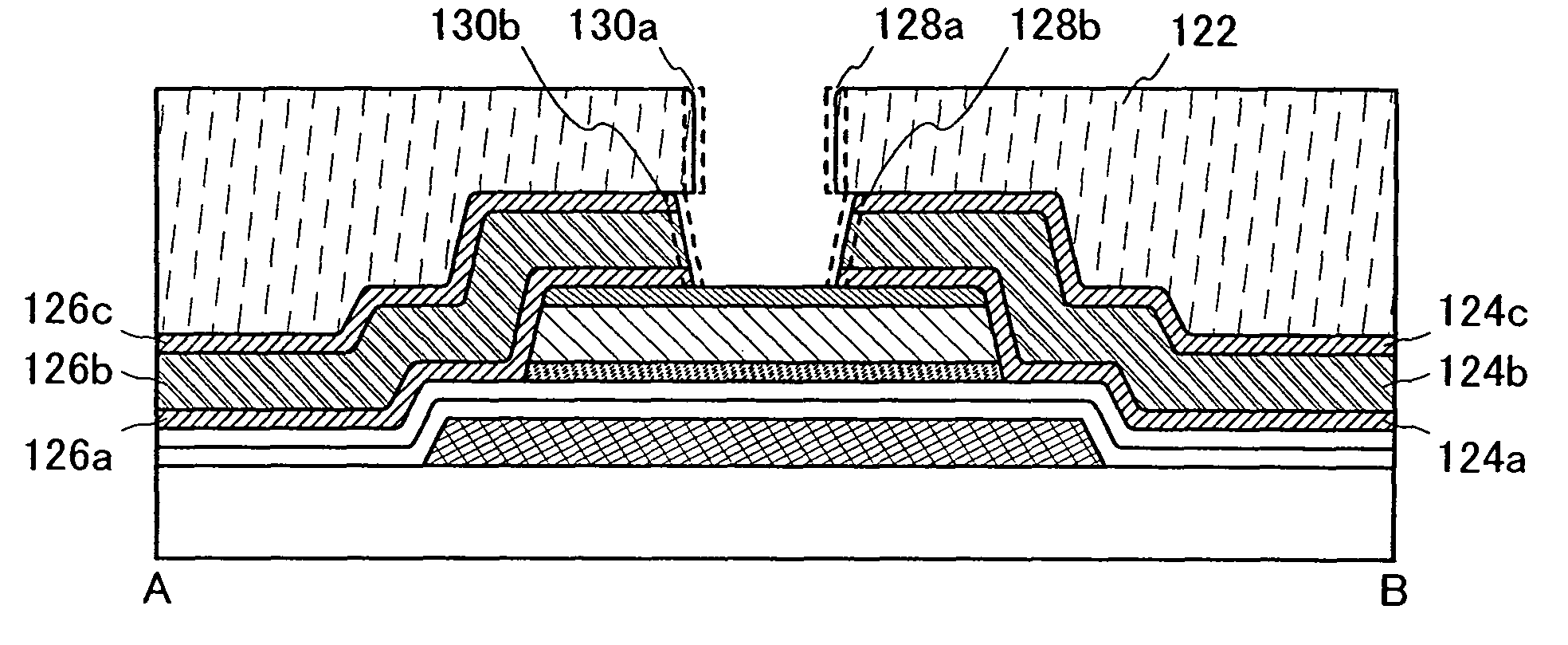
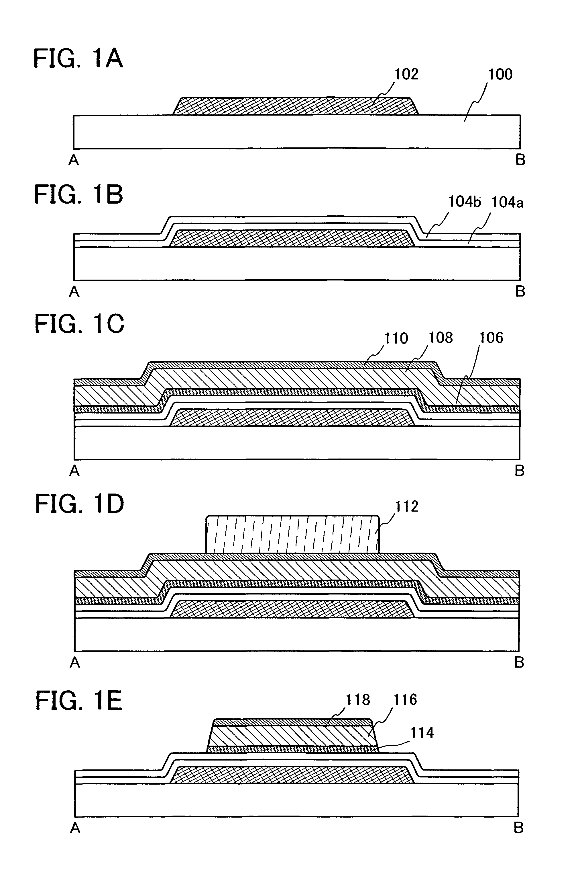
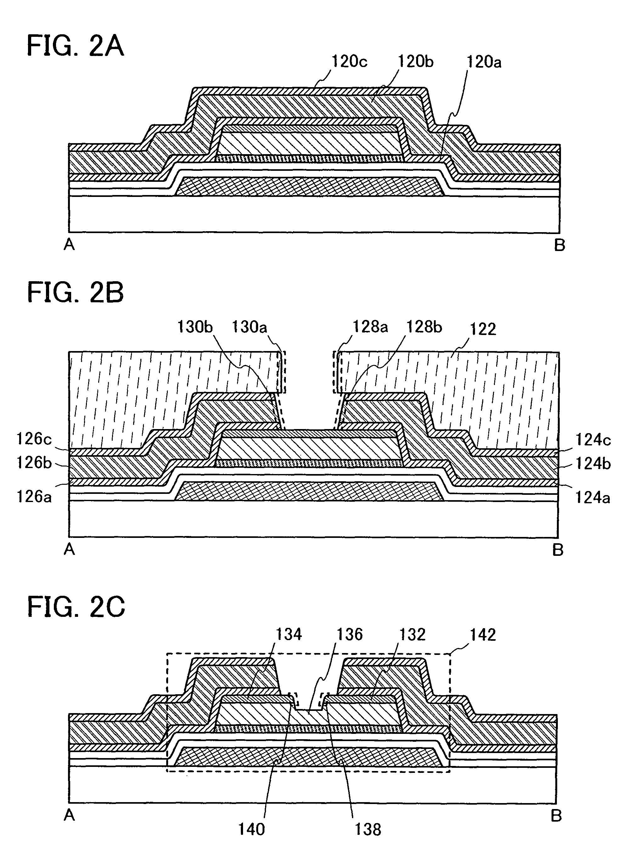
[0053]In this embodiment mode, a manufacturing process of a liquid crystal display device of the present invention, in particular, a manufacturing process of the thin film transistor is described with reference to FIGS. 1A to 1E, FIGS. 2A to 2C, FIGS. 3A to 3C, FIGS. 4A to 4D, FIGS. 5A to 5D, and FIGS. 6A and 6B. FIGS. 1A to 1E, FIGS. 2A to 2C, and FIGS. 3A to 3C are cross-sectional views of the manufacturing process. FIGS. 4A to 4D and FIGS. 5A to 5D are plan views of a connection region of the thin film transistor and a pixel electrode in one pixel. FIGS. 6A and 6B are a plan view and a cross-sectional view of a completed liquid crystal display device.

[0054]Note that various structures can be considered as a plan view structure. This embodiment mode describes typical structures, in which a channel formation region, a source region, and a drain region are arranged linearly (see FIGS. 4A to 4D), and in which a channel formation region and one of a source region and a drain region fo...

embodiment mode 2

[0112]In this embodiment, a manufacturing method of a transistor, in which a microcrystalline semiconductor layer is irradiated with laser beam, so that the crystallinity is improved, with reference to FIGS. 7A to 7D.

[0113]First, a gate electrode is formed over the substrate in the similar manner to Embodiment Mode 1. Then, a gate insulating layer is formed so as to cover a gate electrode (not shown). After that, a microcrystalline semiconductor layer is formed over a gate insulating layer 700 (see FIG. 7A).

[0114]In the above-described manner, when the microcrystalline semiconductor layer is formed over the gate insulating layer 700 by a plasma CVD method or the like, a region which contains many amorphous components (here, such a region is referred to as “an interface region 704”) is formed, in some cases, near the interface between the gate insulating layer 700 and a semiconductor layer 702. In the case where an ultra-thin microcrystalline semiconductor film with a thickness of ab...

embodiment mode 3

[0125]In this embodiment mode, details of a liquid crystal display device including the thin film transistor (hereinafter, also referred to as a “TFT”) shown in Embodiment Modes 1 and 2 is described with reference to FIG. 8, FIG. 9, FIG. 10, FIG. 11, FIG. 12, FIG. 13, FIG. 14, FIG. 15, FIG. 16, FIG. 17, FIG. 18, FIG. 19, FIG. 20, and FIG. 21. The thin film transistor used for the liquid crystal display device illustrated in FIG. 8, FIG. 9, FIG. 10, FIG. 11, FIG. 12, FIG. 13, FIG. 14, FIG. 15, FIG. 16, FIG. 17, FIG. 18, FIG. 19, FIG. 20, and FIG. 21 can be manufactured in the similar manner to the thin film transistor shown in Embodiment Modes 1 and 2.

[0126]First, liquid method crystal display device of a vertical alignment (VA) mode is described. The VA is a kind of mode in which alignment of liquid crystal molecules of a liquid crystal display panel is controlled. The VA liquid crystal display device is a mode in which the major axis of liquid crystal molecules is vertical to a pan...


PUM

PropertyMeasurementUnit
channel widthaaaaaaaaaa

Abstract

It is an object to provide a liquid crystal display device and an electronic device of which aperture ratio increases. The present invention includes a substrate having an insulating surface, a transistor formed over the substrate, a pixel electrode electrically connected to the transistor. The transistor includes a gate electrode, a gate insulating layer over the gate electrode, a semiconductor layer having a microcrystalline structure over the gate insulating layer, and a buffer layer over the semiconductor layer having the microcrystalline structure. The channel width W of the transistor and the channel length L of the transistor satisfy a relation of 0.1≦W / L≦1.7.

Description

BACKGROUND OF THE INVENTION[0001]1. Field of the Invention[0002]The present invention relates to a liquid crystal display device and an electronic device.[0003]2. Description of the Related Art[0004]In recent years, techniques for manufacturing semiconductor devices using a semiconductor thin film which is formed over a substrate having an insulating surface have been researched. Semiconductor devices using the above-mentioned semiconductor thin film are widely used, and in particular, are often used as switching elements for image display devices.[0005]As a switching element of the image display device, an amorphous semiconductor or a polycrystalline semiconductor is used. In the case of using the amorphous semiconductor, since the number of the steps can be reduced by eliminating the steps necessary for crystallization or the like, there is an advantage that the switching element can be manufactured with low cost. In the case of using the polycrystalline semiconductor, there is an...

Claims


Application Information

Patent Timeline
Patent Type & Authority Patents(United States)
IPC IPC(8): G02F1/136
CPCG02F1/1368H01L29/04H01L27/1222H01L29/66765H01L29/78669H01L29/78678H01L29/78696G02F1/133707G02F2201/40H01L29/41733H01L29/4908H01L29/458G02F1/136227H01L27/12H01L27/1214
Inventor KUROKAWA, YOSHIYUKIIKEDA, TAKAYUKIOSADA, TAKESHIINOUE, TAKAYUKI
Owner SEMICON ENERGY LAB CO LTD
Why Eureka
Try Eureka