
Composite dielectric thin film, capacitor and field effect transistor using the same, and each fabrication method thereof

a technology of field effect transistor and composite dielectric thin film, which is applied in the direction of fixed capacitors, nanoinformatics, fixed capacitor details, etc., can solve the problems of degrading reducing the stability of the element, so as to achieve high breakdown voltage characteristics, low leakage current, and high dielectric constant

Inactive Publication Date: 2013-10-15
KOREA INST OF SCI & TECH
View PDF4 Cites 3 Cited by
  • Summary
  • Abstract
  • Description
  • Claims
  • Application Information

AI Technical Summary

Benefits of technology

The composite dielectric thin film exhibits improved leakage current characteristics and high breakdown voltage, enabling stable operation of transistors and capacitors at low voltages, even on plastic substrates, with a dielectric constant of 15 or higher, suitable for flexible electronic applications.

Problems solved by technology

Development of such flexible transistor has a restriction that the temperature of a fabrication process should be very low in consideration of stability of temperature at which a plastic substrate can tolerate.
If a low voltage driving transistor is fabricated by forming a thin gate insulating film on the rough substrate, a pin hole would be easily formed in the fabrication process or an insulation breakdown occurs at a low voltage due to a non-uniform step coverage, shortening the long life span and degrading stability of the element.

Method used


Image

  • Composite dielectric thin film, capacitor and field effect transistor using the same, and each fabrication method thereof
  • Composite dielectric thin film, capacitor and field effect transistor using the same, and each fabrication method thereof
  • Composite dielectric thin film, capacitor and field effect transistor using the same, and each fabrication method thereof

Examples


embodiment 1

[0067][Embodiment 1] (Ba0.6Sr0.4TiO3)1-x—(MgO)x (x=0.1˜0.3) Composite Dielectric Thin Film Using a PLD Method and Fabrication of Capacitor Using the Same

[0068]First, in order to prepare powder having a composition of Ba0.6Sr0.4TiO3, powder of BaCO3, SrCO3, TiO2 was weighted according to a composition ratio of Ba0.6Sr0.4TiO3, and the weighted powder of BaCO3, SrCO3, TiO2 was mixed in an ethanol solvent through ball milling for 24 hours. At this time, zirconia ball was used in performing ball milling. In a Ba0.6Sr0.4TiO3 dielectric, as the ratio of [Ba] and [Sr], other composition ratio than that of 0.6:0.4 used in this embodiment may be used, and there is no restriction to a particular composition ratio. Subsequently, the mixed powder was dried and thermally treated at 1200° C. for three hours to synthesize Ba0.6Sr0.4TiO3 powder.

[0069]Thereafter, 10 mol %, 20 mol %, and 30 mol % of MgO was added to the synthesized Ba0.6Sr0.4TiO3 powder, on which zirconia ball milling was performed fo...

embodiment 2

[0075][Embodiment 2] (Ba0.6Sr0.4TiO3)1-x—(MgO)x (x=0.2˜0.3) Composite Dielectric Thin Film Using a Sputtering Method and Fabrication of Capacitor Using the Same

[0076]After Ba0.6Sr0.4TiO3 powder was synthesized in the same manner as in the above-described Embodiment 1, to which 20 mol % and 30 mol % of MgO were added, respectively. Zirconia ball milling was performed on the resultant material for 24 hours, and then, mixing, drying, molding and thermally treating process were performed to obtain a 2-inch ceramic target having a composition of (Ba0.6Sr0.4TiO3)1-x—(MgO)x (x=0.2˜0.3). Finally, the ceramic target was sintered at 1400° C. for five hours to complete the fabrication of a sputtering target.

[0077]Next, a composite dielectric thin film having a thickness of 300 nm was formed at a room temperature by using the obtained target having the composition of (Ba0.6Sr0.4TiO3)1-x—(MgO)x (x=0.2˜0.3). At this time, RF power was 80W, the process pressure was changed from 10 mTorr to 60 mTor...

embodiment 3

[0084][Embodiment 3] (Bi1.5Zn1.0Nb1.5O7)1-x—(MgO)x (x=0.1˜0.3) Composite Dielectric Thin Film Using the PLD Method and Fabrication of Capacitor Using the Same

[0085]First, in order to prepare powder having a composition of Bi1.5Zn1.0Nb1.5O7, powder of Bi2O3, ZnO, Nb2O5 was weighted according to a composition ratio of Bi1.5Zn1.0Nb1.5O7, and the weighted Bi2O3, ZnO, Nb2O5 powder was mixed in an ethanol solvent through ball milling for 24 hours. At this time, zirconia ball was used for the ball milling. Subsequently, the mixed powder was dried and thermally treated at 900° C. for three hours to synthesize Bi1.5Zn1.0Nb1.5O7.

[0086]Next, 10 mol %, 20 mol % and 30 mol % of MgO were added to the synthesized Bi1.5Zn1.0Nb1.5O7 powder, respectively, on which zirconia ball milling was performed for 24 hours. The resultant material was mixed, dried, molded and thermally treated to fabricated 1-inch ceramic target having a composition of (Bi1.5Zn1.0Nb1.5O7)1-x—(MgO)x (x=0.1˜0.3). Finally, the cera...


PUM

PropertyMeasurementUnit
temperatureaaaaaaaaaa
driving voltageaaaaaaaaaa
thicknessaaaaaaaaaa

Abstract

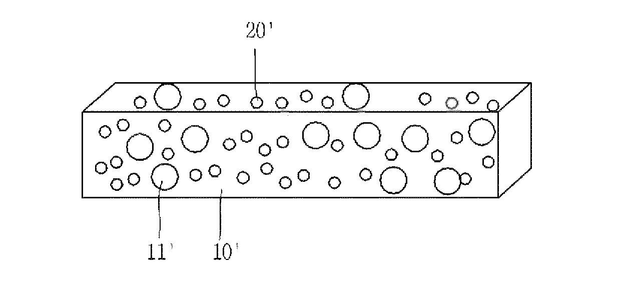
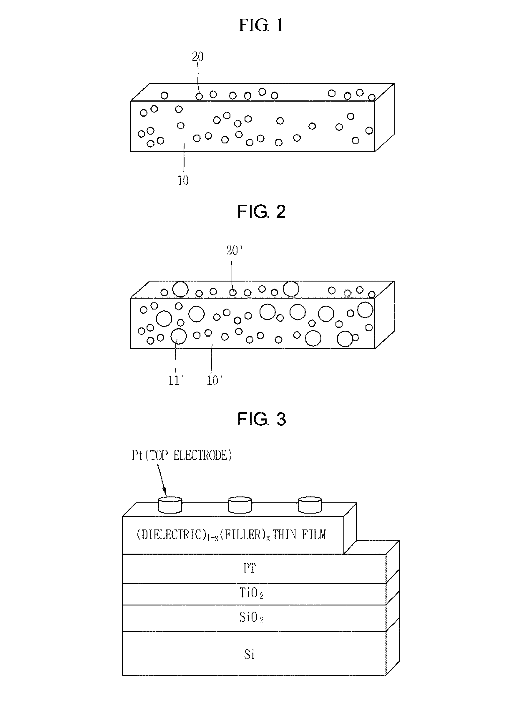
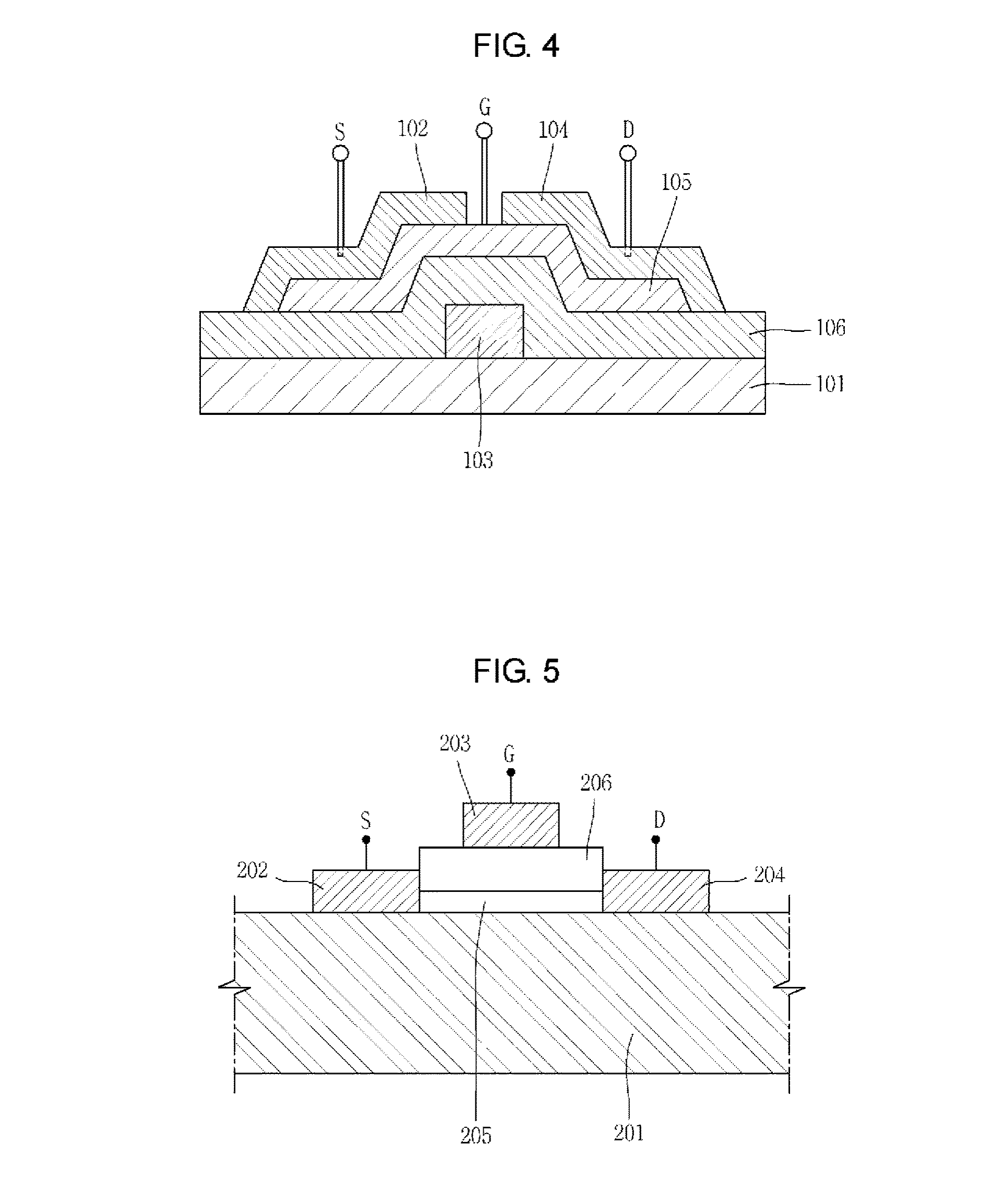
a composite dielectric thin film capable of high dielectric constant, low leakage current characteristics, and high dielectric breakdown voltage while being deposited at a room temperature, a capacitor and a field effect transistor (FET) using the same, and their fabrication methods. The composite dielectric thin film is deposited at a room temperature or less than 200° C. and comprises crystalline or amorphous insulating filler uniformly distributed within an amorphous dielectric matrix or within an amorphous and partially nanocrystalline dielectric matrix.

Description

BACKGROUND OF THE INVENTION[0001]1. Field of the Invention[0002]The present invention relates to a composite dielectric thin film capable of high dielectric constant, low leakage current characteristics, and high dielectric breakdown voltage while being deposited at a room temperature, a capacitor and a field effect transistor (FET) using the same, and their fabrication methods.[0003]2. Description of the Related Art[0004]Recently, development of a transistor using oxide semiconductor (ZnO, In2O3, SnO2, InGaZnO4, and the like) as a channel layer (which is also referred to as a ‘channel region’, hereinafter) has been actively progressing. In particular, research on application of oxide semiconductor to a flexible electronic element and a transparent display based on the excellent semiconductor properties is ongoing.[0005]Development of such flexible transistor has a restriction that the temperature of a fabrication process should be very low in consideration of stability of temperatu...

Claims


Application Information

Patent Timeline
Patent Type & Authority Patents(United States)
IPC IPC(8): H01L29/78H01G4/06C23C14/34C09D1/00
CPCB82Y10/00C23C14/08H01G4/085H01G4/1209H01G4/1218H01G4/1254H01G4/20H01G4/33H01L21/02194H01L21/02266H01L28/40H01L28/55H01L29/4908H01L29/7869H10K10/472H10K10/478H01L21/31604
Inventor KIM, IL-DOOKIM, DONG-HUNKIM, HO-GICHO, NAM-GYU
Owner KOREA INST OF SCI & TECH
Learn More