
Semiconductor device comprising multilayer dielectric film and related method

a dielectric film and semiconductor technology, applied in semiconductor devices, capacitors, electrical devices, etc., can solve the problems of reducing the dielectric constant, degrading the leakage current characteristics of zirconium oxide single films, and increasing the leakage current of capacitors including tantalum oxide layers, etc., to achieve excellent heat resistance, low leakage current characteristics, and high dielectric constant

Active Publication Date: 2012-02-07
SAMSUNG ELECTRONICS CO LTD
View PDF21 Cites 2 Cited by
  • Summary
  • Abstract
  • Description
  • Claims
  • Application Information

AI Technical Summary

Benefits of technology

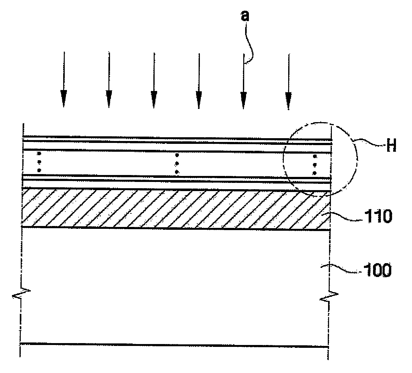
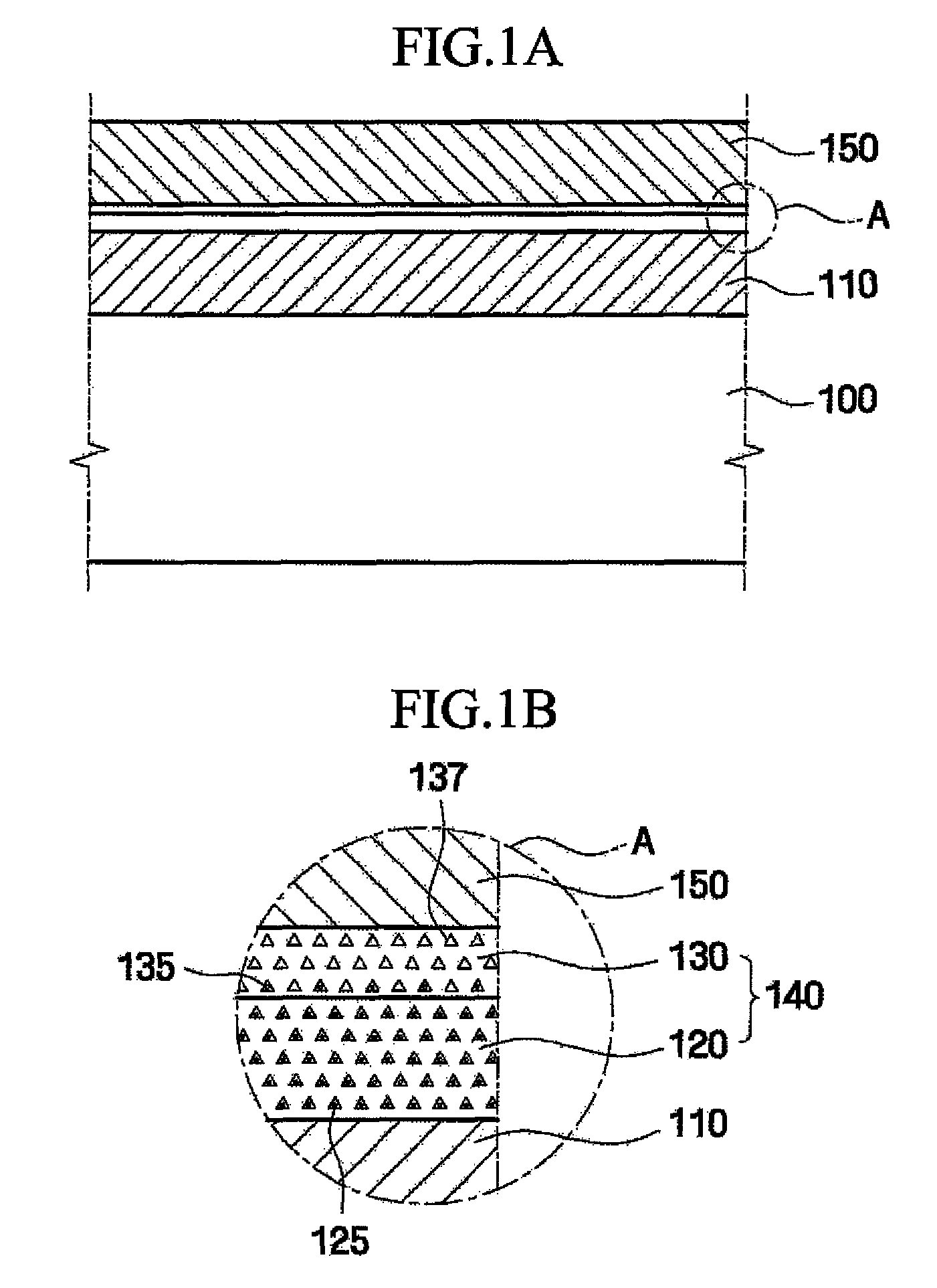
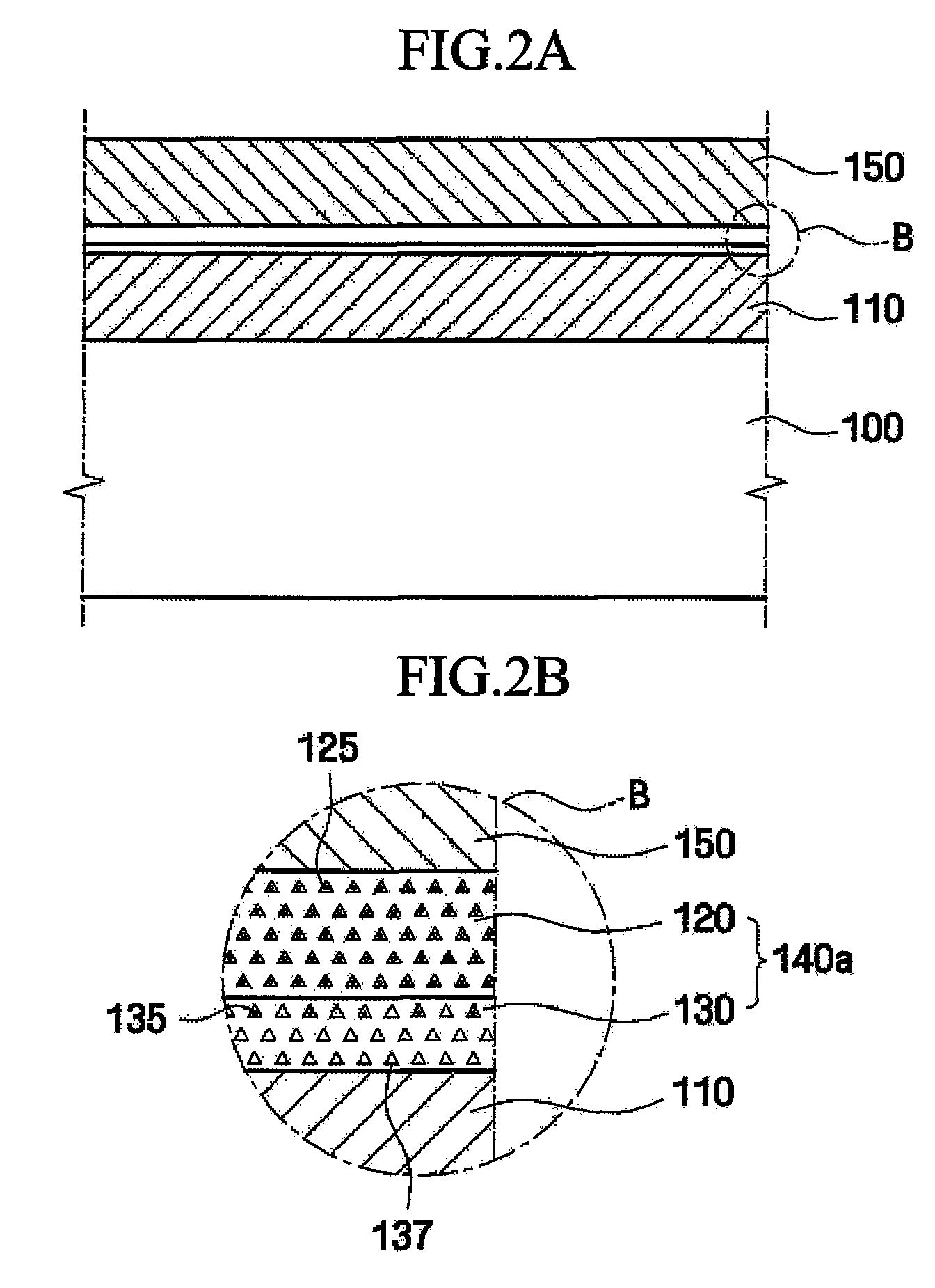
[0008]Embodiments of the invention provide a semiconductor device comprising a multilayer dielectric film having a tetragonal crystalline structure, wherein the multilayer dielectric film has a relatively high dielectric constant, relatively low leakage current characteristics, and excellent heat resistance. Embodiments of the invention also provide a method for fabricating a semiconductor device comprising the multilayer dielectric film having a tetragonal crystalline structure.

Problems solved by technology

Also, the heat generated during a subsequent process will reduce the dielectric constant and degrade the leakage current characteristics of a zirconium oxide single film.
A tantalum oxide layer has a relatively high dielectric constant in a crystalline state; however, a high temperature heat treatment at a temperature of 700° C. or more needs to be performed on the tantalum oxide layer, and the high temperature heat treatment increases the leakage current of a capacitor including the tantalum oxide layer.
A tetragonal system hafnium oxide has a higher dielectric constant than a zirconium oxide film; however, it is undesirable to use a hafnium oxide in a tetragonal system crystalline state to fabricate a dielectric film of a semiconductor device because it is difficult to shape a hafnium oxide in a tetragonal system crystalline state into a thin film.

Method used


Image

  • Semiconductor device comprising multilayer dielectric film and related method
  • Semiconductor device comprising multilayer dielectric film and related method
  • Semiconductor device comprising multilayer dielectric film and related method

Examples


experimental example 1

[0072]FIG. 10 illustrates XRD patterns of a zirconium oxide single film and a multilayer dielectric film in accordance with an embodiment of the invention.

[0073]Referring to FIG. 10, the XRD pattern of the zirconium oxide single film is the same as the XRD pattern of the zirconium oxide single film having a tetragonal crystalline structure. The crystalline structure may be confirmed through analysis of peaks of the XRD pattern of the zirconium oxide single film using an X-ray diffractometer. In addition, when a thickness ratio of the zirconium oxide film and the hafnium oxide film was 2:1 or more, the XRD pattern of the multilayer dielectric film was the same as the XRD pattern of the zirconium oxide single film. When a thickness ratio of the zirconium oxide film and the hafnium oxide film was 1:1, an m(−111) peak was additionally found. In this case, the multilayer dielectric film does not have a tetragonal crystalline structure but a monoclinic crystalline structure. That is, in t...

experimental example 2

[0074]FIGS. 11A and 11B are graphs showing breakdown voltage (V) as a function of equivalent oxide thickness for a known zirconium oxide single film and a multilayer dielectric film in accordance with an embodiment of the invention.

[0075]Referring to the graph of FIG. 11A, the X-axis represents equivalent oxide thickness (Toxeq) of the zirconium oxide single film and the multilayer dielectric film, and the Y-axis represents a breakdown voltage (BV) when a leakage current of 1 fA per unit cell flows by application of a positive voltage. As shown in FIG. 11A, the zirconium oxide single film had a breakdown voltage of about 1.05 V and the multilayer dielectric film had a breakdown voltage of about 1.17 V with respect to the same equivalent oxide thickness of 5.7 Å. That is, the breakdown voltage of the multilayer dielectric film in accordance with an embodiment of the invention was about 0.12 V higher than the breakdown voltage of the single film with respect to the same equivalent oxi...

experimental example 3

[0077]FIG. 12 is a graph showing leakage current density as a function of applied voltage for a known zirconium oxide single film and a multilayer dielectric film in accordance with an embodiment of the invention.

[0078]Referring to the graph of FIG. 12, the X-axis represents applied voltage, and the Y-axis represents leakage current density. Leakage current density is the amount of leakage current flowing per unit cell. In this example, the respective equivalent oxide thicknesses of the zirconium oxide single film and the multilayer dielectric film were each 5.7 Å. As shown in FIG. 12, when the leakage current density was 1 fA, the applied voltage of the zirconium oxide single film was 1.05 V / −0.90 V, and the applied voltage of the multilayer dielectric film was 1.17 V / −1.02 V. That is, the applied voltage of the multilayer dielectric film was greater than that of the zirconium oxide single film by about 0.12 V on the positive side and was less than that of the zirconium oxide singl...


PUM

PropertyMeasurementUnit
temperatureaaaaaaaaaa

Abstract

A semiconductor device including a multilayer dielectric film and a method for fabricating the semiconductor device are disclosed. The multilayer dielectric film includes a type-one dielectric film having a tetragonal crystalline structure, wherein the type-one dielectric film comprises a first substance. The multilayer dielectric film also comprises a type-two dielectric film also having a tetragonal crystalline structure, wherein the type-two dielectric film comprises a second substance different from the first substance and a dielectric constant of the type-two dielectric film is greater than a dielectric constant of the type-one dielectric film.

Description

CROSS-REFERENCE TO RELATED APPLICATIONS[0001]This is a divisional of application Ser. No. 12 / 034,868 filed on Feb. 21, 2008, which claims priority to Korean Patent Application No. 10-2007-0018409, filed on Feb. 23, 2007. The subject matter of both of these applications is hereby incorporated by reference in their entirety.BACKGROUND OF THE INVENTION[0002]1. Field of the Invention[0003]Embodiments of the invention relate to a semiconductor device and a method for fabricating the semiconductor device. In particular, embodiments of the invention relate to a semiconductor device comprising a multilayer dielectric film and a method for fabricating the semiconductor device.[0004]2. Description of the Related Art[0005]The degree of integration of semiconductor devices has increased in recent years. Accordingly, the respective amounts of chip area available for components of semiconductor devices have been reduced. A capacitor, which is used to store information in a DRAM device, is one suc...

Claims


Application Information

Patent Timeline
Patent Type & Authority Patents(United States)
IPC IPC(8): H01L21/02
CPCH01L28/40H01L27/10852H10B12/033H10B99/00H10B12/00
Inventor KANG, SANG-YEOLLEE, JONG-CHEOLLIM, KI-VINCHOI, HOON-SANGCHUNG, EUN-AE
Owner SAMSUNG ELECTRONICS CO LTD
Learn More