Doping of semiconductor materials by nuclear transmutation

a technology of nuclear transmutation and semiconductor materials, applied in semiconductor devices, chemical to radiation conversion, electrical apparatus, etc., can solve the problems of reducing the quality of the resultant doped layer, reducing reducing the efficiency of the doping method, etc., to achieve the effect of improving the quality of the resultant doped layer, reducing the risk of ion implantation and diffusion, and highly undesirable effects

Active Publication Date: 2013-01-29
THE UNITED STATES OF AMERICA AS REPRESENTED BY THE SECRETARY OF THE NAVY
View PDF10 Cites 4 Cited by
  • Summary
  • Abstract
  • Description
  • Claims
  • Application Information

AI Technical Summary

Benefits of technology

[0017]An additional advantage of the present invention over implantation and diffusion lies in the superior quality of the resultant doped layer. Because of the uniformity of the cross section over a range of beam energies, the present invention's doping via 3He transmutation produces a relatively thick and relatively uniform doped layer in the material. In contrast, according to diffusion, the bulk of the dopants will inevitably be near the surface through which they enter, and a density gradient will occur through the thickness. Ion implantation produces more uniform layers than does diffusion, but requires implanting at multiple energies to produce thick layers; this is because the implantation profile is a function of both the stopping power of the target material and the initial ion beam energy.
[0018]In the present invention's 16O (3He, 4He) 15O reaction, the transmutation and decay process ultimately produces atomic nitrogen (N), as opposed to molecular nitrogen (N2). N2 complexes are energetically stable and can be highly unpredictable in their electronic behavior. Due to their stability, N2 complexes are very difficult to anneal once they are in the material and, as such, are highly undesirable. Thus, in order to avoid these stable complexes, it is generally important in practice of this inventive genre to use sources of atomic nitrogen, rather than sources of molecular nitrogen, for doping electronic materials.
[0019]The inventive methodology is and will be a viable option for existing and newly discovered materials. Traditional methodologies such as ion implantation and diffusion will remain an option for newly discovered materials, but will require significant study and improvement in order to minimize defect production and optimize material performance. While annealing is possible for most materials, higher temperatures make extensive annealing very costly, especially in terms of mass production of devices.
[0020]3He (also referred to herein as “helium three” or “helium-3”) is an isotope of helium that contains two protons and one neutron. 3He occurs in nature much more rarely than the most prevalent isotope of helium, namely, 4He (also referred to as “helium four” or “helium-4”), ...

Problems solved by technology

Great difficulty has been encountered in conventional approaches to doping semiconductor films (e.g., ZnO films) to produce p-type material.
This difficulty is largely associated with donor-like defects (e.g., oxygen vacancies and zinc interstitials in ZnO material) that easily form during deposition or processing.
As distin...

Method used


Image

  • Doping of semiconductor materials by nuclear transmutation
  • Doping of semiconductor materials by nuclear transmutation
  • Doping of semiconductor materials by nuclear transmutation

Examples


Embodiment Construction

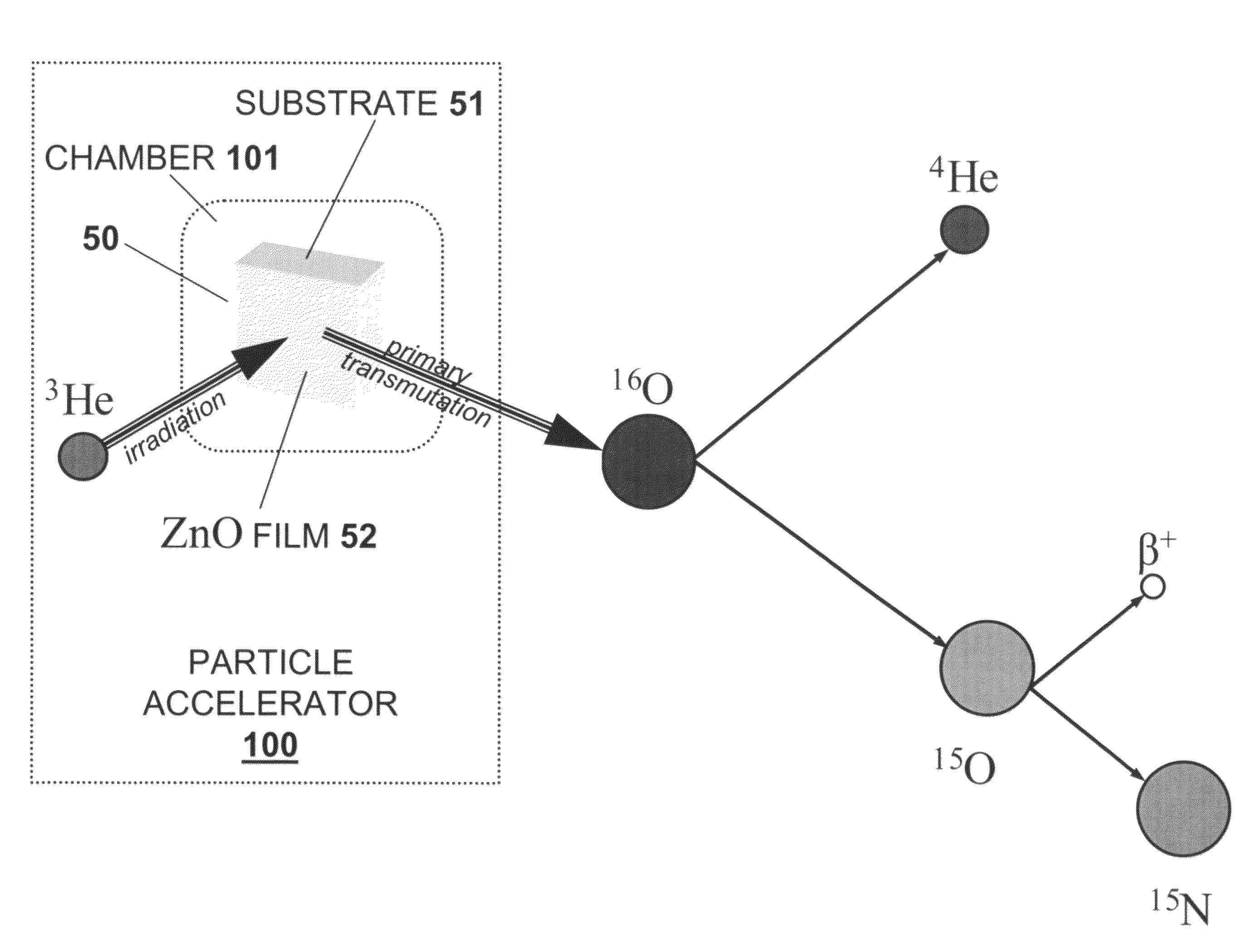
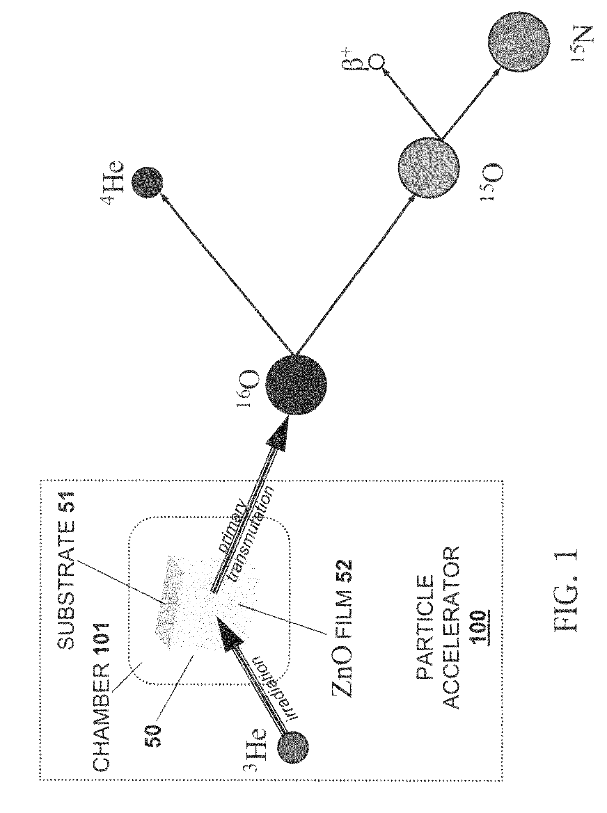
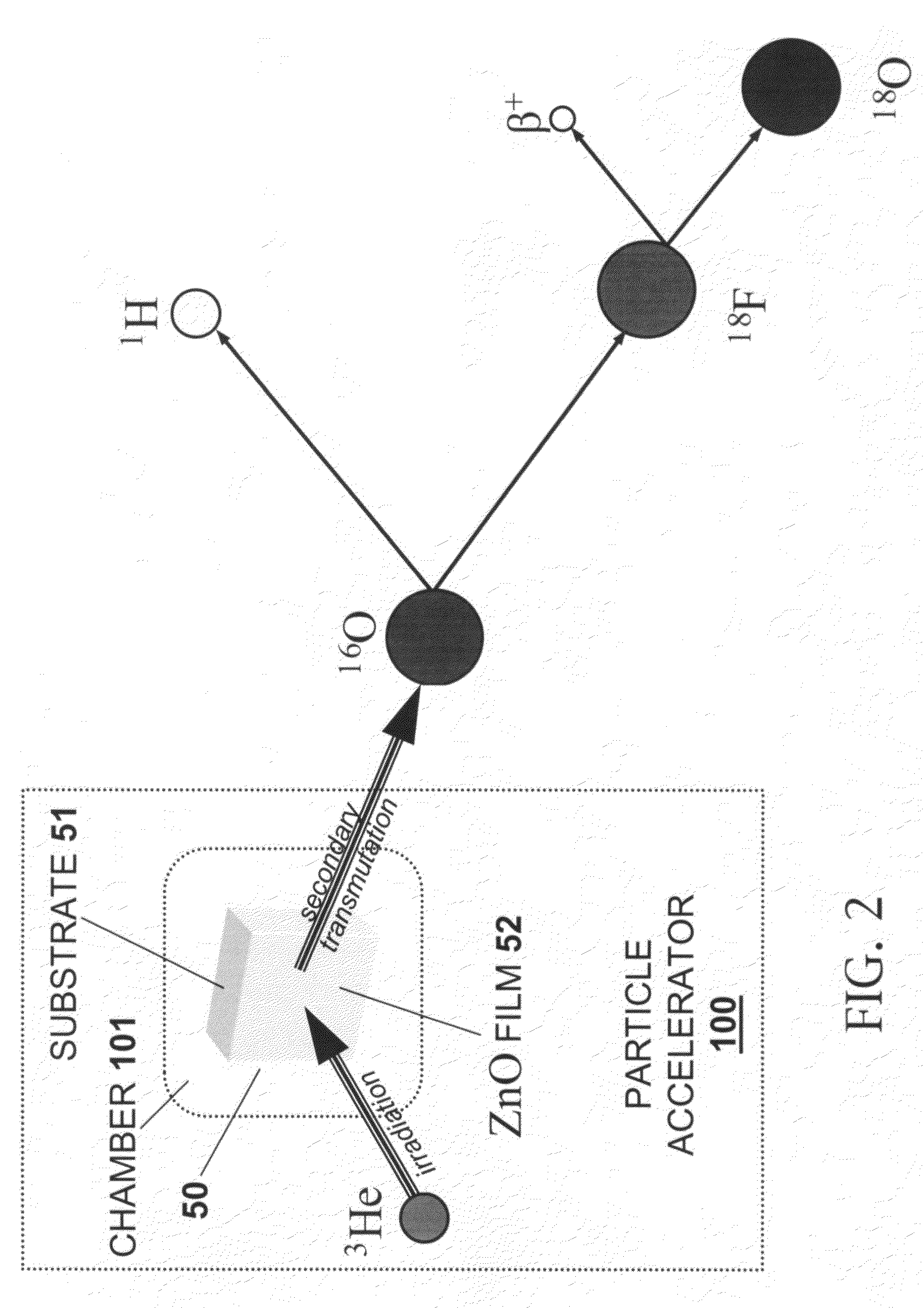
[0035]In its basic principle, the present invention effects nuclear transmutation doping (NTD), according to which a nuclear reaction is induced using an energetic ion incident on a lattice atom, thereby producing an atom of a different species in the material. The present invention uniquely features the utilization of high energy 3He ion beams to bring about nuclear transmutation of materials.

[0036]Of particular interest to the present inventors is their novel use of high energy 3He ion beams to effectuate nuclear transmutation of zinc oxide, whereby nitrogen is produced from a reaction with oxygen in a crystalline ZnO thin film. As elaborated upon hereinbelow, the present inventors successfully tested this mode of inventive practice and found that, vis-à-vis the original zinc oxide films, the inventively doped zinc oxide films were significantly different in terms of resistivity, photoconductivity, scanning electron microscopy, cathodoluminescence, and ion beam analysis. Of partic...


PUM


Abstract

As typically embodied, the inventive method features bombardment of atomic nuclei with 3He ions in order to effect transmutation of atoms from a first atomic element to a second atomic element. Two notable inventive genres describe transmutation of: oxygen to nitrogen in an oxygen-containing target (e.g., including ZnO film); and, carbon to boron in a carbon-containing target (e.g., including SiC film). According to the former, transmutation of 16O to 15N occurs; more specifically, transmutation of 16O to 15O occurs via nuclear bombardment, and then transmutation of 15O to 15N occurs via decay by positron emission. According to the latter, transmutation of 12C to 11B occurs; more specifically, transmutation of 12C to 11C occurs via nuclear bombardment, and then transmutation of 11C to 11B occurs via decay by positron emission. Inventive practice frequently results in significant alteration of at least one physical property among: electronic carrier concentration; resistivity; photoconductivity; luminescence; morphology.

Description

CROSS-REFERENCE TO RELATED APPLICATIONS[0001]This application claims the benefit of U.S. provisional patent application No. 60 / 867,223, filing date 27 Nov. 2006, hereby incorporated herein by reference, invention title “Doping of Oxygen- and Carbon-Containing Materials by Nuclear Transmutation Using High Energy 3-He Ion Beams,” joint inventors Noel A. Guardala, Ian Patrick Wellenius, Jack L. Price, John F. Muth.STATEMENT OF GOVERNMENT INTEREST[0002]The invention described herein may be manufactured and used by or for the Government of the United States of America for governmental purposes without payment of any royalties thereon or therefor.BACKGROUND OF THE INVENTION[0003]The present invention relates to semiconductor materials, more particularly to methods and systems for doping or otherwise changing the physical character of semiconductor materials.[0004]Conventional doping methodologies include (i) ion implantation, (ii) diffusion, and (iii) incorporating dopant atoms during the...

Claims


Application Information

Patent Timeline
IPC IPC(8): G21G1/10
CPCH01L21/261H01L29/22H01L29/1608H01L21/42G21G1/10
Inventor GUARDALA, NOEL A.WELLENIUS, IAN PATRICKPRICE, JR., JACK L.MUTH, JOHN F.
Owner THE UNITED STATES OF AMERICA AS REPRESENTED BY THE SECRETARY OF THE NAVY
Why Eureka
Try Eureka