Hierarchial power map for low power design

a low-power circuit and hierarchy technology, applied in the field of computer-implemented methods for debugging low-power circuit design, can solve the problems of inefficient and error-prone designers to debug the entire chip, become more and more complex and difficult to debug, and achieve the effect of easy debugging

Active Publication Date: 2013-01-29
SYNOPSYS INC
View PDF2 Cites 14 Cited by
  • Summary
  • Abstract
  • Description
  • Claims
  • Application Information

AI Technical Summary

Benefits of technology

[0013]An object of this invention is to provide a solution to display low power information in a graphic window called power map having the low power information visible at the top level of the power map, which will help user to understand the power structure and the relationship between power network design and circuit design quickly for easy debugging, wherein the power map includes power domains, isolation cells, level shifters, power switches and power supplies.
[0014]One embodiment in the present invention is to provide a computer-implemented method for generating and displaying a power map, which is a power schematic diagram in a graphic window to show the low power network design based on the low power information defined in a power format in top level, to allow designers to debug the low power network design and its associated circuit design, in which the power map comprises a plurality of power domain symbols to represent power domains and to link to the associated parts of the circuit design.
[0017]A feature of the power map, which is displayed in a graphic window, is that it provides some active annotation to easily communicate and interact with users. Accordingly, it is more user friendly to let users debug power network together with digital circuit design in an interactive interface.

Problems solved by technology

For example of a system-on-chip (SoC) design, it becomes more and more complex and harder to debug as more and more digital circuit design and low power network design are integrated into one chip.
Since traditional hardware description languages (HDL) are not adequate to specify the power design information, power format, such as UPF, provides a format without touching the existing HDL codes.
As a result, it is inefficient and error prone for the designers to debug the entire chip if low power network design can not be viewed in the top level to interact with the power designer; therefore it is important to have a user graphic interface having the power network design in the top level while the associated digital design is viewable under power domains, so that the entire design can be viewed with main debugging focused on the power network design.

Method used


Image

  • Hierarchial power map for low power design
  • Hierarchial power map for low power design
  • Hierarchial power map for low power design

Examples


Embodiment Construction

[0029]The detailed explanation of the present invention is described as following. The described preferred embodiments are presented for purposes of illustrations and descriptions, and they are not intended to limit the scope of the present invention.

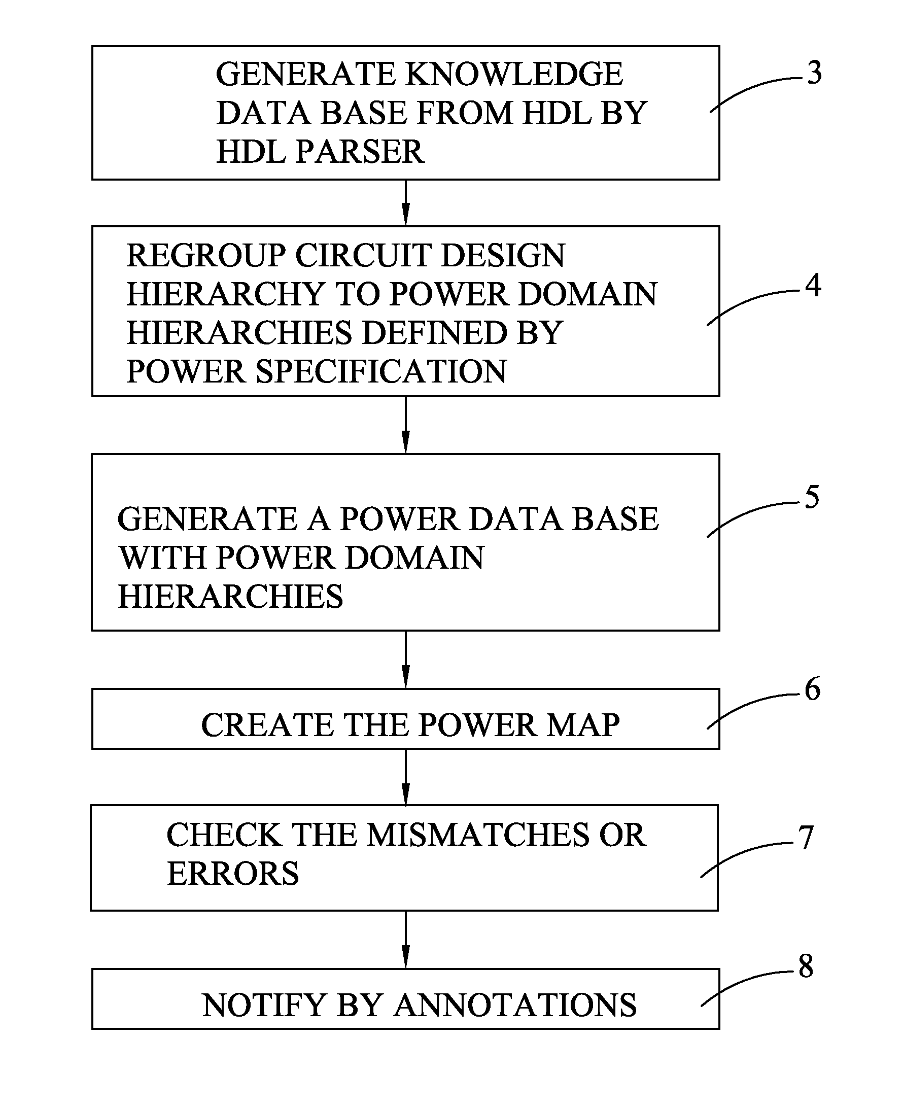
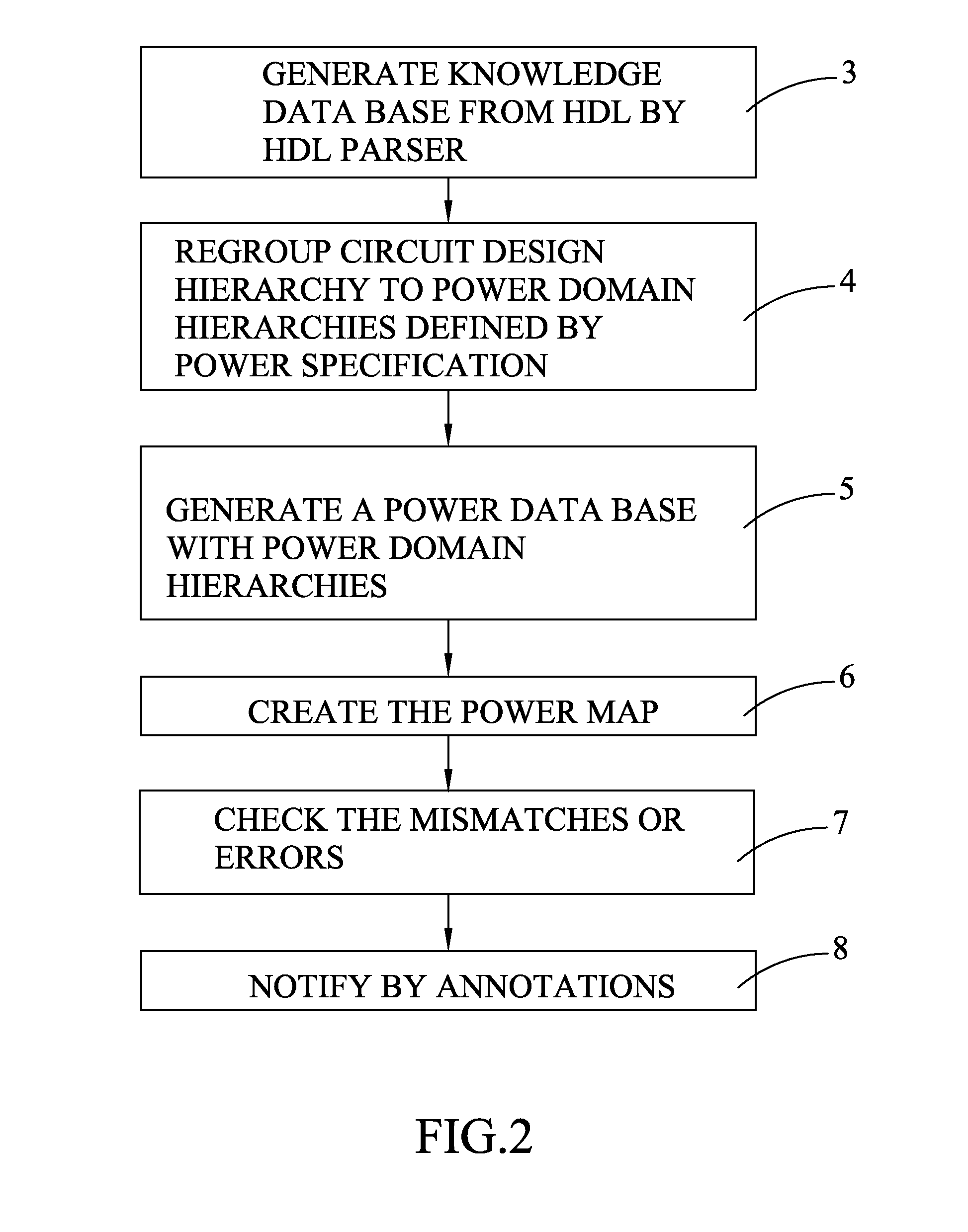
[0030]In one embodiment, the computer-implemented method for creating the power map of this invention comprises the following steps as shown in FIG. 2. In step 3, the original text-based circuit design HDL codes are parsed and transformed into internal structure and stored in a knowledge data base. The knowledge data base is an internal computer-readable data structure, which is generally hierarchical structure but not limited in hierarchical or flattened structure, of the circuit design and could easily be manipulated by software, and the knowledge base can be generated by a HDL parser. In step 4, power designs specified in CPF or UPF are parsed and transformed into internal structure by a CPF or UPF parser. After that, the original ci...


PUM


Abstract

A computer-implemented method for debugging the power aspect of an IC design by integrating the power specification expressed in certain power specification format and its corresponding circuit design within a power schematic diagram called power map. Power map is created by using a power data base generated by regrouping the original circuit design hierarchy to new hierarchies defined by the power specification. Power map contains power cell symbols (such as isolation cells, level shifters, power switches) and signal nets, and can show the relationship between power domains. Power map can also display mismatches or errors between the power specification and the circuit design for those signals connecting the power domains. Furthermore, power map can be used in conjunction with simulation result.

Description

CROSS REFERENCE TO RELATED APPLICATIONS[0001]This application claims the benefit of priority of U.S. Provisional Application No. 61 / 358,002, filed Jun. 24, 2010, and titled “Method and system for displaying IC design intent with power domain intent,” the contents of which are herein incorporated by reference in its entirety.BACKGROUND OF THE INVENTION[0002]1. Field of the Invention[0003]The present invention relates to a computer-implemented method for debugging low power circuit design in the field of integrated circuit (IC) design, and in particular, to a method for creating an integrated graphic user interface to debug the entire IC design including both logic circuit design and the associated low power network design.[0004]2. Description of the Related Art[0005]With the rapid progress of mobile devices and consumer electronic equipments during recent years, there are more applications such as smart cellular phones, personal mobile computers, MP3 audio players, notebooks and digi...

Claims


Application Information

Patent Timeline
Patent Type & Authority Patents(United States)
IPC IPC(8): G06F9/455G06F17/50
CPCG06F17/5022G06F2217/78G06F30/33G06F2119/06
Inventor HSU, CHIH-NENGLIN, I-LIANGFENG, WEN-CHI
Owner SYNOPSYS INC
Why Eureka
Try Eureka