Optical sensor device, display apparatus, and method for driving optical sensor device

a technology of optical sensor and display device, which is applied in the direction of optical radiation measurement, static indicating device, instruments, etc., can solve the problems of touch sensor not being stably operated, touch position may be erroneously detected or detection sensitivity may vary, display quality of display panel may be degraded, etc., to achieve the effect of appropriate detection sensitivity and not degrading display quality

Active Publication Date: 2013-02-05
SOLAS OLED LTD
View PDF28 Cites 87 Cited by
  • Summary
  • Abstract
  • Description
  • Claims
  • Application Information

AI Technical Summary

Benefits of technology

[0010]The invention can advantageously provide an optical sensor device comprising optical sensors two-dimensionally arranged on a substrate, the optical sensor device enabling the adverse effect, on the detection sensitivity of the optical sensors, of time degradation and temperature changes in the optical sensors, and also provide a method for driving the optical sensor device. Furthermore, the invention can advantageously provide a display apparatus comprising display pixels two-dimensionally arranged on a substrate and optical sensors also two-dimensionally arranged on the substrate, the display apparatus allowing the optical sensors to achieve appropriate detection sensitivity without degrading display quality.

Problems solved by technology

Thus, if such a thin-film transistor is used as a touch sensor, a touch position may be erroneously detected or detection sensitivity may vary.
Thus, the touch sensor may fail to operate stably.
Thus, the display quality of the display panel may be degraded.
Furthermore, if the sensors and the interconnects connected to the sensors are arranged so as to avoid degrading the display quality, a sufficient number of optical sensors cannot be arranged.
Hence, appropriate detection sensitivity cannot be achieved.
Thus, it is difficult for the optical sensors to achieve appropriate detection sensitivity without degrading the display quality.

Method used


Image

  • Optical sensor device, display apparatus, and method for driving optical sensor device
  • Optical sensor device, display apparatus, and method for driving optical sensor device
  • Optical sensor device, display apparatus, and method for driving optical sensor device

Examples


first embodiment

[0046]First, the invention will be described.

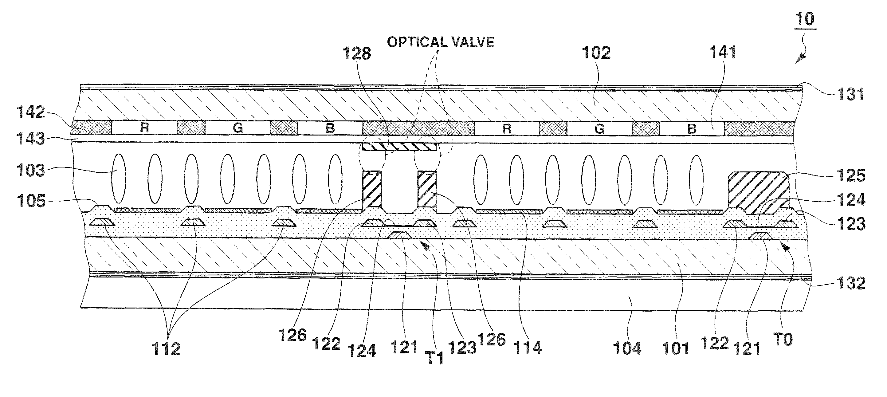
[0047]FIG. 1 is a diagram showing an example of the cross-sectional structure of a display panel 10 comprising an optical sensor device according to a first embodiment of the invention.

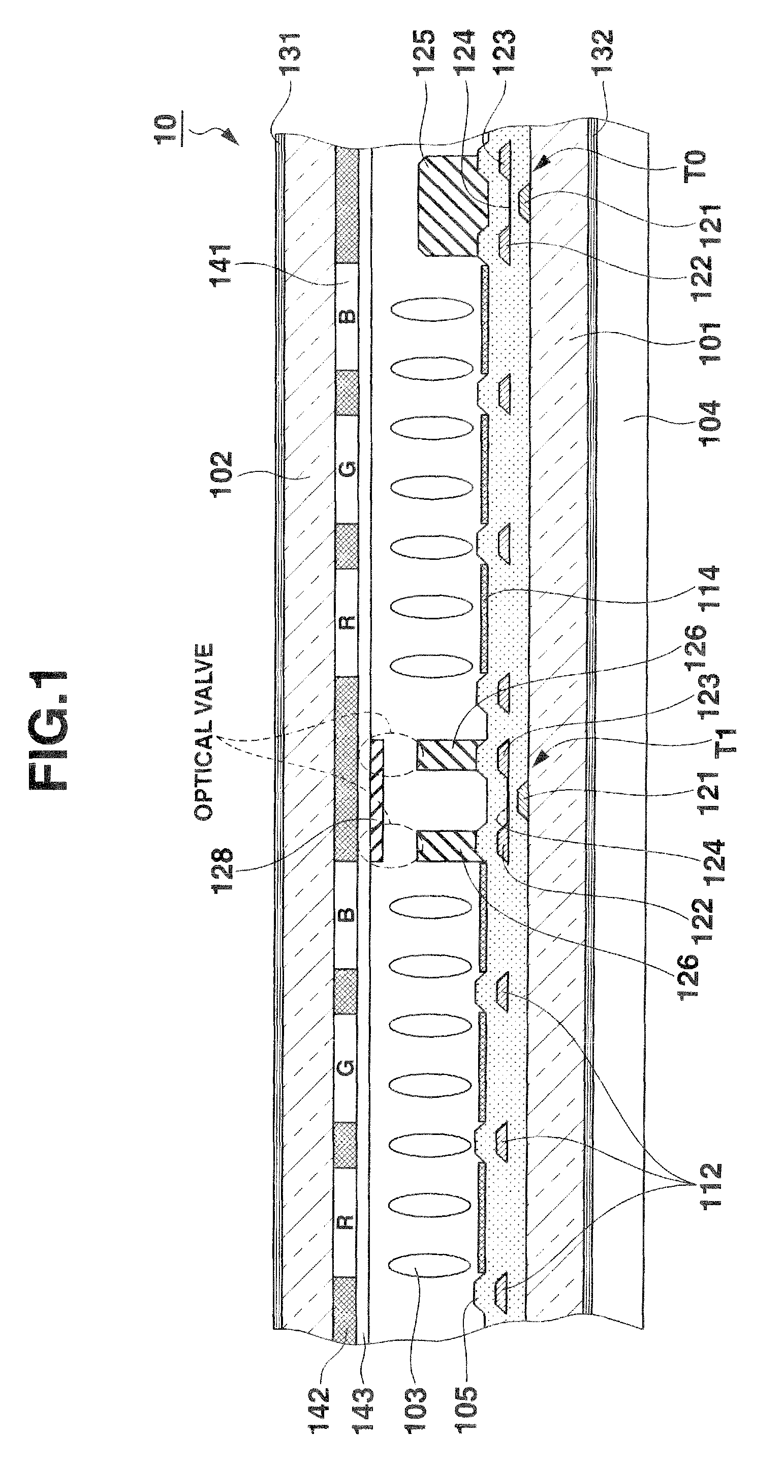
[0048]FIG. 2 is a diagram showing a configuration of a TFT sensor T0 provided in the display panel 10.

[0049]FIGS. 3A and 3B are diagrams showing a configuration of a TFT sensor T1 provided in the display panel 10. FIG. 3A shows that a user's finger or the like is not touching the display panel 10. FIG. 3B shows that the user's finger or the like is touching the display panel 10.

[0050]FIG. 4 is a front view of the display panel comprising the optical sensor device according to the first embodiment of the invention.

[0051]FIG. 1 is a cross-sectional view of the display panel 10 taken along direction I-I shown in FIG. 4.

[0052]The display panel 10 shown in FIG. 1 includes built-in plural optical sensor units of the thin-film transistor type and forms a liquid cr...

second embodiment

[0206]Now, the invention will be described.

[0207]FIG. 13 is a front view showing an example of a display panel 10 comprising an optical sensor device according to a second embodiment of the invention.

[0208]The display panel 10 shown in FIG. 13 forms a liquid crystal display apparatus with built-in optical sensors of the thin-film-transistor type. Components of the display panel 10 which are equivalent to those shown in FIG. 4 are denoted by the same reference numbers. Description of these components is omitted or simplified.

[0209]Like the display panel 10 according to the first embodiment, the display panel 10 according to the present embodiment comprises display pixels including three subpixels corresponding to color filters 141 for the three colors, red (R), green (G), and blue (B). The display pixels are two-dimensionally arranged.

[0210]The optical sensor device according to the present embodiment includes optical sensors of the thin-film-transistor type comprising TFT sensors T0...

third embodiment

[0252]Now, the invention will be described.

[0253]FIG. 17 is a front view showing an example of a display panel 10 comprising an optical sensor device according to a third embodiment of the invention.

[0254]The display panel 10 in FIG. 17 forms a liquid crystal display apparatus with built-in optical sensors of the thin-film-transistor type. Here, components of the display panel 10 which are equivalent to those shown in FIG. 4 are denoted by the same reference numbers. Description of these components is omitted or simplified.

[0255]Like the display panels 10 according to the first and second embodiments, the display panel 10 according to the present embodiment comprises display pixels including three subpixels corresponding to color filters 141 for the three colors, red (R), green (G), and blue (B). The display pixels are two-dimensionally arranged.

[0256]As is the case with the first embodiment, the optical sensor device according to the present embodiment includes optical sensors of t...


PUM


Abstract

An optical sensor device includes a plurality of optical sensor units two-dimensionally arranged, a scan driver, and a detection driver. The scan driver sets optical sensor units, in each row, in a selected state. The detection driver acquires detection signals corresponding to illuminance of incident light on the optical sensor units. Each of the optical sensor units comprises a first optical sensor including a first photoelectric conversion section blocked from light and a second optical sensor including a second photoelectric conversion section configured to change the illuminance in response to an externally applied external force. The detection driver maintains each voltage of electrodes of the first optical sensors and each voltage of electrodes of the second optical sensors in equal voltage levels to each other, and acquires a plurality of voltage signals in parallel.

Description

CROSS-REFERENCE TO RELATED APPLICATIONS[0001]This application is based upon and claims the benefit of priority from prior Japanese Patent Applications No. 2010-083740, filed Mar. 31, 2010; No. 2010-083743, filed Mar. 31, 2010; and No. 2010-265380, filed Nov. 29, 2010, the entire contents of all of which are incorporated herein by reference.BACKGROUND OF THE INVENTION[0002]1. Field of the Invention[0003]The invention relates to an optical sensor device, a display apparatus, and a method for driving the optical sensor device, and in particular, to an optical sensor device suitable for a two-dimensional sensor such as a touch panel built into a display apparatus, and a method for driving the optical sensor device.[0004]2. Description of the Related Art[0005]An optical sensor made by a thin-film transistor (an optical sensor of a thin-film transistor type) detects a photoelectric current signal resulting from incidence of light on the optical sensor with a predetermined potential (norma...

Claims


Application Information

Patent Timeline
Patent Type & Authority Patents(United States)
IPC IPC(8): G06F3/038G09G5/00
CPCG06F3/0412G06F3/0421G02F1/13338G02F1/13613H01L31/10
Inventor YAMAMOTO, TAKUMI
Owner SOLAS OLED LTD
Why Eureka
Try Eureka