Liquid crystal display device

a liquid crystal display and display device technology, applied in semiconductor devices, optics, instruments, etc., can solve problems such as image quality degradation, and achieve the effect of suppressing the generation of optical leak current and reducing the required alignment accuracy

Active Publication Date: 2013-02-26
JAPAN DISPLAY INC +1
View PDF9 Cites 3 Cited by
  • Summary
  • Abstract
  • Description
  • Claims
  • Application Information

AI Technical Summary

Benefits of technology

[0009]Here, in case of the thin film transistor shown in FIG. 9A and FIG. 9B, the semiconductor film is not completely shielded from light radiated from the backlight by the gate electrode and hence, an optical leak current is generated whereby there exists a possibility that image quality is deteriorated. On the other hand, in case of the thin film transistor shown in FIG. 10A and FIG. 10B, although the generation of an optical leak current can be suppressed, since it is necessary to arrange the semiconductor film inside the gate electrode, the required alignment accuracy becomes strict. Although the required strict alignment accuracy can be alleviated by increasing a width of the gate electrode, for example, this increase of the width of the gate electrode lowers a numerical aperture.
[0010]The invention has been made in view of such drawbacks, and it is an object of the invention to provide a liquid crystal display device having thin film transistors which can alleviate the required alignment accuracy of a semiconductor film while suppressing the generation of an optical leak current.
[0019]According to the invention, it is possible to provide a liquid crystal display device having thin film transistors which can alleviate the required alignment accuracy in forming the semiconductor film while suppressing the generation of an optical leak current.

Problems solved by technology

Here, in case of the thin film transistor shown in FIG. 9A and FIG. 9B, the semiconductor film is not completely shielded from light radiated from the backlight by the gate electrode and hence, an optical leak current is generated whereby there exists a possibility that image quality is deteriorated.

Method used


Image

  • Liquid crystal display device
  • Liquid crystal display device
  • Liquid crystal display device

Examples


first embodiment

[First Embodiment]

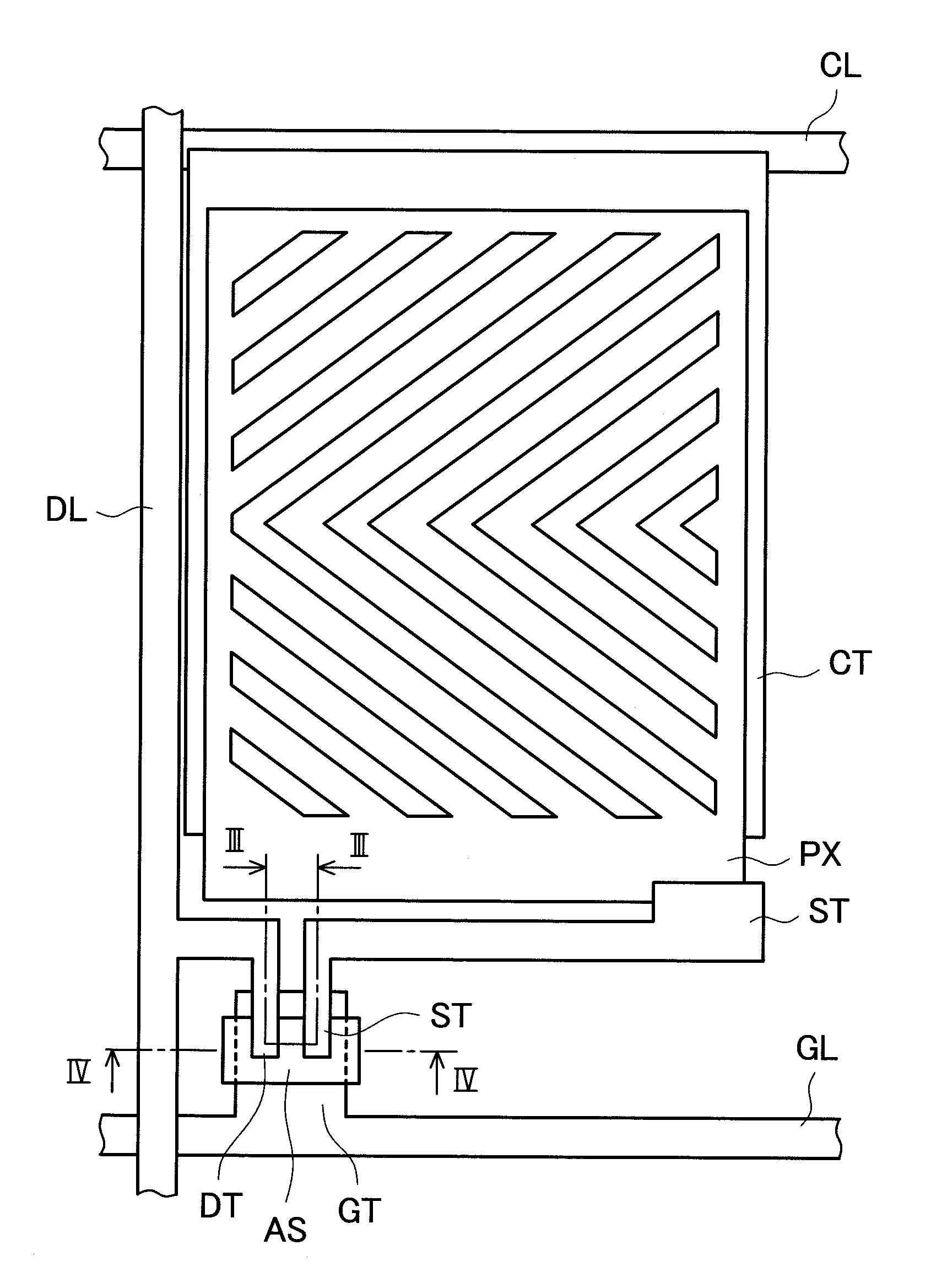
[0032]Hereinafter, a first embodiment of the invention is explained in conjunction with drawings. A display device according to this embodiment is an IPS (In-Plane Switching)-type liquid crystal display device. The liquid crystal display device includes: a TFT substrate on which scanning signal lines (gate signal lines), video signal lines (drain signal lines), thin film transistors, pixel electrodes, and counter electrodes are arranged; a color filter substrate which faces the TFT substrate in an opposed manner and forms color filters thereon; liquid crystal material which is hermetically filled in a region sandwiched between both substrates; and a backlight which supplies light to the TFT substrate and the color filter substrate. The TFT substrate is configured such that the thin film transistors are arranged on a transparent substrate made of glass or the like in a matrix array.

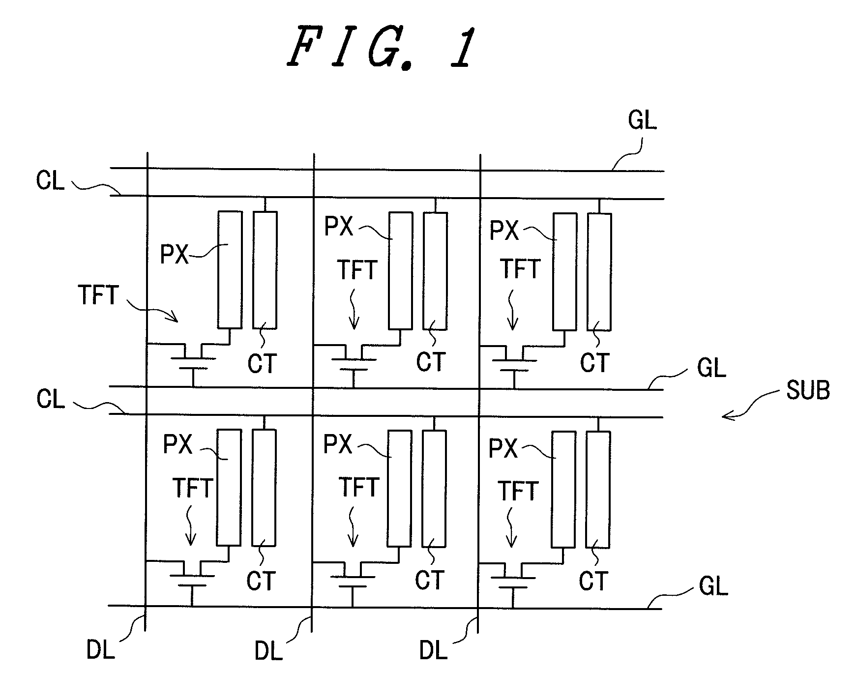
[0033]FIG. 1 is a view showing an equivalent circuit of the TFT substrate SUB of the ...

second embodiment

[Second Embodiment]

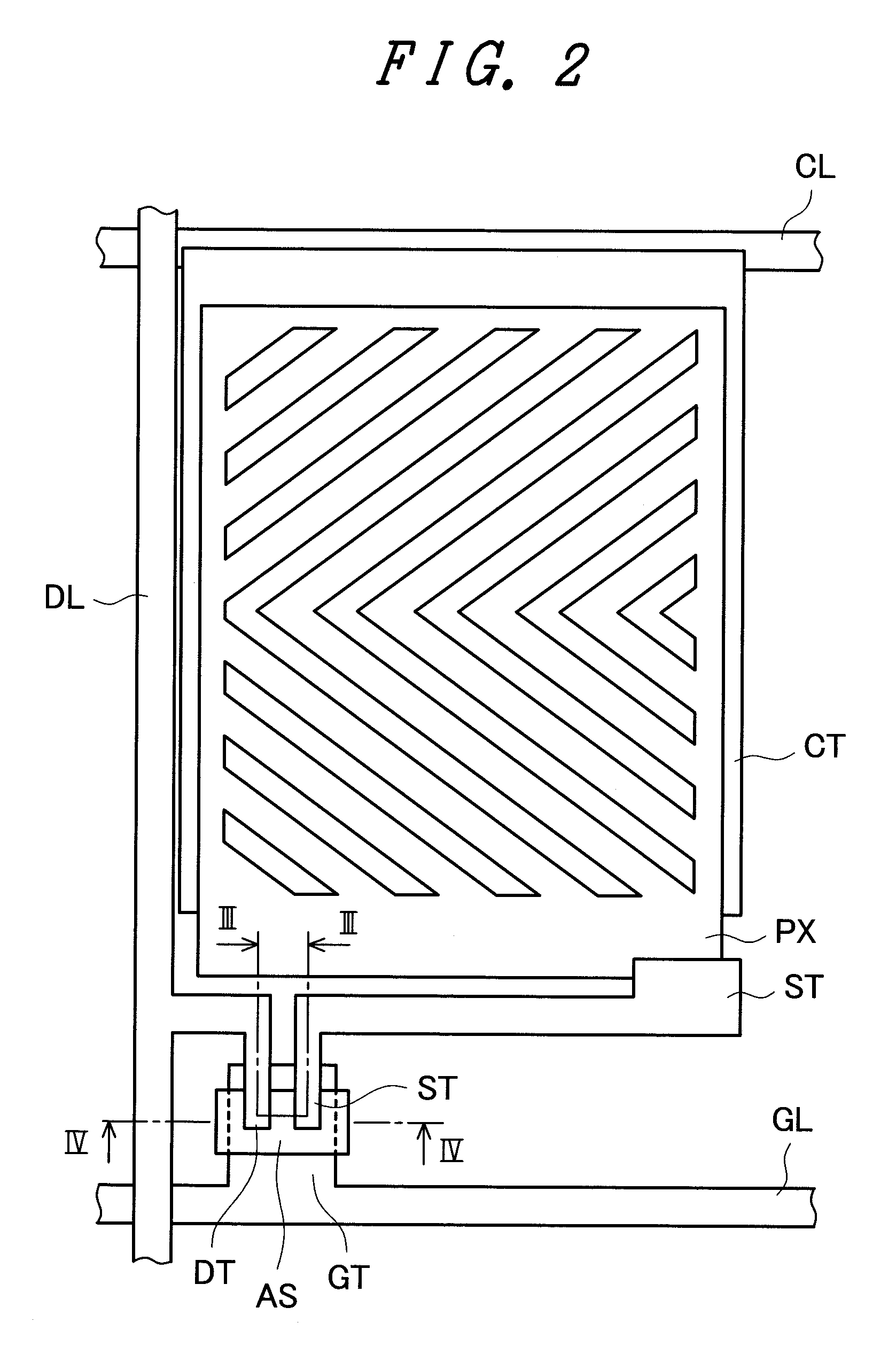
[0052]In the above-mentioned first embodiment, as shown in FIG. 2, the gate electrode GT is formed at a position away from the video signal line DL on a right side in the drawing, and the drain electrode DT is formed in a rightwardly projecting manner from the video signal line DL in the drawing. The drain electrode DT which projects from the video signal line DL is bent so as to extend along the gate electrode GT and is connected to the first region of the semiconductor film AS after passing the extending portion of the gate electrode GT. However, the second embodiment differs from the first embodiment with respect to a point that an area where a gate electrode GT and a video signal line DL overlap with each other in plan view is provided, and the video signal line DL is connected with the first region of the semiconductor film AS as a drain electrode DT. Although the second embodiment is explained hereinafter, the explanation of the constitutions which are subst...


PUM

PropertyMeasurementUnit
crystal particle sizeaaaaaaaaaa
transparentaaaaaaaaaa

Abstract

A liquid crystal display device having thin film transistors which can alleviate the required alignment accuracy of a semiconductor film while suppressing the generation of an optical leak current is provided. The liquid crystal display device includes: a transparent substrate; gate electrodes which are stacked above the transparent substrate; source electrodes and drain electrodes which are stacked above the gate electrodes; and semiconductor films each of which is stacked above the gate electrode and controls an electric current between the source electrode and the drain electrode based on an electric field generated by the gate electrode, wherein the semiconductor film is formed into a planar shape, and includes a first region which overlaps with the gate electrode in plane and a second region which does not overlap with the gate electrode in plane, and the source electrode and the drain electrode are not connected to the semiconductor film in the second region, and are connected to the semiconductor film in the first region.

Description

[0001]The present application claims priority from Japanese application JP 2009-159169 filed on Jul. 3, 2009, the content of which is hereby incorporated by reference into this application.BACKGROUND OF THE INVENTION[0002]1. Field of the Invention[0003]The present invention relates to a liquid crystal display device which displays an image by allowing light from a backlight to pass through a substrate on which thin film transistors (TFTs) are formed.[0004]2. Description of the Related Art[0005]In a liquid crystal display device, there has been known an active-matrix-type liquid crystal display device which performs a display control of pixels using thin film transistors (TFTs). Such a liquid crystal display device is constituted of a liquid crystal panel including a TFT substrate on which thin film transistors are formed in a matrix array, and a backlight which supplies light to the liquid crystal panel.[0006]As the device structure of the thin film transistor, there has been a bott...

Claims


Application Information

Patent Timeline
Patent Type & Authority Patents(United States)
IPC IPC(8): G02F1/1368
CPCG02F1/1368H01L27/124H01L29/42384H01L29/41733
Inventor SAKAI, TAKESHI
Owner JAPAN DISPLAY INC
Why Eureka
Try Eureka