Apparatus and method to tolerate floating input pin for input buffer

a floating input pin and buffer technology, applied in the field of integrated circuit pull-up and pull-down circuitry for input/output pads, can solve the problems of increasing the power consumption of the device, unpredictability of the operation of input buffer circuitry connected to the pad, and damage to the input buffer circuitry, so as to achieve the effect of saving power and high speed operation

Active Publication Date: 2013-03-19
MACRONIX INT CO LTD
View PDF6 Cites 6 Cited by
  • Summary
  • Abstract
  • Description
  • Claims
  • Application Information

AI Technical Summary

Benefits of technology

[0018]A first state in the latch turns on the pass transistor to electrically couple the pad to the reference voltage. A second state in the latch turns off the pass transistor to electrically decouple the pad from the reference voltage. The circuitry coupled to the latch is responsive to an initialization event to establish the first state in the latch. Establishing the first state in the latch turns on the pass transistor to electrically couple the pad to the first voltage and “pre-charge” the pad. This prevents the pin from floating following the initialization event, and thus ensures that the input buffer circuitry is in a known state following the initialization event. The initialization event may be for example, a power-up event of the device, or any other event which could lead to an indeterminate floating voltage on the pad.
[0020]By turning off the pass transistor when the pad is being driven by internal or external drivers, the load of the “pre-charge” current path through the pass transistor is removed, saving power and allowing higher speed operation.

Problems solved by technology

During operation, if an I / O pad is left “floating”, meaning that the pad is not being driven to a known voltage by external or internal drivers, the pad may float at a voltage level sufficient to cause input buffer circuitry connected to the pad to turn-on and operate unpredictably.
This unpredictable operation increases power consumption for the device and may cause damage to the input buffer circuitry.
A floating voltage on the pad may also place the input buffer circuitry in an indeterminate state, resulting in indeterminate signals propagating to the internal circuitry of the device and causing oscillations and other spurious effects.
These indeterminate signals can cause oscillations and other spurious effects in the internal circuitry of the device 100.
The cross-bar current can damage the input buffer circuitry 110 and cause failure of the device 100.
One drawback to the use of resistive pull-up or pull-down circuits 130, 140 is that they consume significant amounts of power when the pad 105 is driven to a voltage level opposite that of the self-biased voltage level provided by the circuits 130, 140.
Another drawback is that the current path through the resistive pull-up or pull-down circuits 130, 140 loads the pad 105 when the pad 105 is being driven by the output buffer circuitry 120, which impacts the output transient time of the device 100.

Method used


Image

  • Apparatus and method to tolerate floating input pin for input buffer
  • Apparatus and method to tolerate floating input pin for input buffer
  • Apparatus and method to tolerate floating input pin for input buffer

Examples


first embodiment

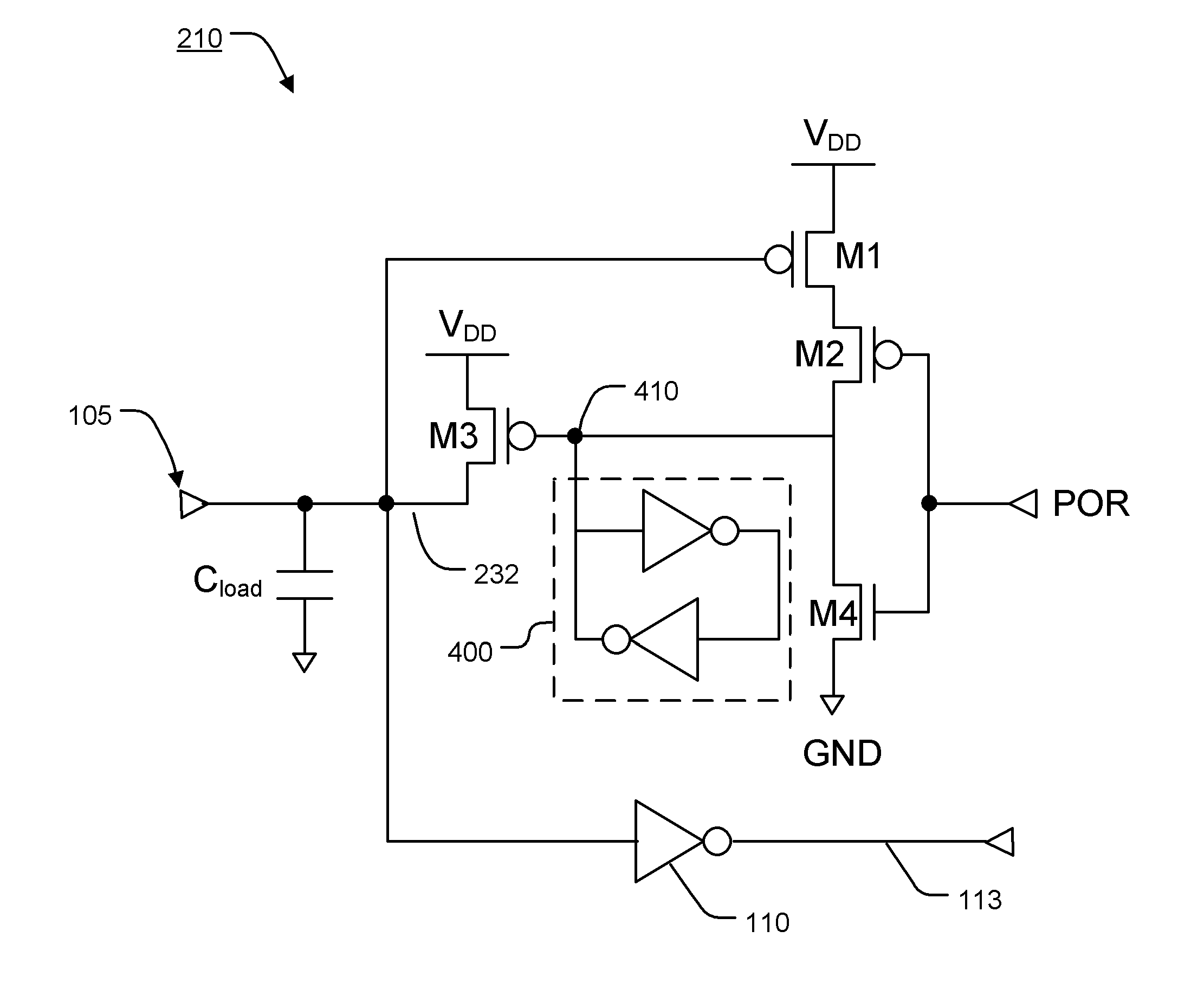
[0044]FIG. 4 illustrates the input buffer circuitry 210 for the integrated circuit device 200. As shown in FIG. 4, the input buffer circuitry 210 includes PMOS pass transistor M3 having a first conduction terminal connected to the output terminal 232, a second conduction terminal connected to a reference voltage (VDD in this example), and a control terminal coupled to a terminal of the latch circuit 400 at node 410. The pass transistor M3 is turned-on and off to selectively couple the output terminal 232 to reference voltage VDD, depending upon whether the state of the latch 400 is low or high.

[0045]The latch 400 can be implemented using a pair of cross-coupled invertors. Alternatively, other circuits may be used to implement the latch 400.

[0046]FIG. 5 illustrates an embodiment of a timing diagram for operating the architecture of FIG. 4 using the methods described herein. As will be understood the timing diagram of FIG. 5 is simplified and not necessarily to scale.

[0047]The sequenc...

second embodiment

[0056]FIG. 6 illustrates the input buffer circuit 210 used to pre-charge the pad to a low reference voltage (ground in this example) in response to the initialization event, and monitoring the voltage on the pad to detect a change indicating the pad is being pulled high.

[0057]As shown in FIG. 6, the input buffer circuit 210 includes an NMOS pass transistor M6 having a first conduction terminal connected to the output terminal 232, a second conduction terminal coupled to ground, and a control terminal coupled to latch circuit 400 at node 610. The pass transistor M6 is turned on and off to selectively couple the output terminal 232 to ground, depending upon whether the state of the latch is high or low.

[0058]FIG. 7 illustrates an embodiment of a timing diagram for operating the architecture of FIG. 6 using the methods described herein. As will be understood the timing diagram of FIG. 7 is simplified and not necessarily to scale.

[0059]In response to the initialization event at time T1,...


PUM


Abstract

An integrated circuit device includes a pad adapted to receive a signal from an internal or external driver, and an input buffer circuit including an input terminal coupled to the pad. The input buffer circuit includes a pass transistor having a control terminal, a first conduction terminal connected to the pad, and a second conduction terminal connected to a first voltage. The input buffer circuit also includes a latch having a terminal electrically coupled to the control terminal of the pass transistor. The input buffer circuit further includes circuitry coupled to the latch, the circuitry including a feedback transistor having a control terminal electrically coupled to the pad, a first conduction terminal electrically coupled to a second voltage, and a second conduction terminal coupled to the latch.

Description

BACKGROUND OF THE INVENTION[0001]1. Field of the Invention[0002]The present invention relates generally to integrated circuits, and more particularly to pull-up and pull-down circuitry for input / output pads of integrated circuits.[0003]2. Description of Related Art[0004]Integrated circuits include input / output (I / O) pads used for receiving and transmitting signals. During operation, if an I / O pad is left “floating”, meaning that the pad is not being driven to a known voltage by external or internal drivers, the pad may float at a voltage level sufficient to cause input buffer circuitry connected to the pad to turn-on and operate unpredictably. This unpredictable operation increases power consumption for the device and may cause damage to the input buffer circuitry. A floating voltage on the pad may also place the input buffer circuitry in an indeterminate state, resulting in indeterminate signals propagating to the internal circuitry of the device and causing oscillations and other ...

Claims


Application Information

Patent Timeline
Patent Type & Authority Patents(United States)
IPC IPC(8): H03K3/00
CPCH03K19/0002H03K3/00H03K19/09425
Inventor HUNG, CHUN-HSIUNGCHANG, KUEN-LONGKUO, NAI-PINGCHIH, HSIEH-MING
Owner MACRONIX INT CO LTD
Why Eureka
Try Eureka