However, a simple proportional shrink is not always possible because of what are known as “short channel effects.” Short channel effects are particularly acute when channel length under a transistor gate is comparable in magnitude to depletion depth of an operating transistor, and can include reduction in threshold voltage, severe surface scattering, drain induced barrier lowering (DIBL), source / drain punch through, and electron mobility issues.
Unfortunately, while such implants improve some electrical characteristics such as threshold voltage rolloff and drain induced barrier lowering, the resultant increased channel doping can adversely affect electron mobility and reduce channel transconductance, primarily because of the increased dopant scattering in the channel.
Unfortunately, creating a suitable insulator layer is expensive and difficult to accomplish.
Modern SOI technology can use silicon wafers, but tends to require expensive and time consuming additional wafer processing steps to make an insulative silicon oxide layer that extends across the entire wafer below a surface layer of device-quality single-crystal silicon.
Both BOX formation and layer transfer, however, tend to be costly manufacturing techniques with a relatively high failure rate.
Accordingly, manufacture of SOI transistors is not an economically attractive solution for many leading manufacturers.
Factors including cost of transistor redesign to cope with “floating body” effects, the need to develop new SOI specific transistor processes, and other circuit changes is added to SOI wafer costs, render these solutions undesirable in many situations.
But again, like SOI transistors, while moving to a radically new transistor architecture solves some short channel effect issues, it creates others, often requiring even more significant transistor layout redesign than SOI.
Considering the likely need for complex non-planar transistor manufacturing techniques to make a finFET, and the unknown difficulty in creating a new process flow for finFET, manufacturers have been reluctant to invest in semiconductor fabrication facilities capable of making finFETs.
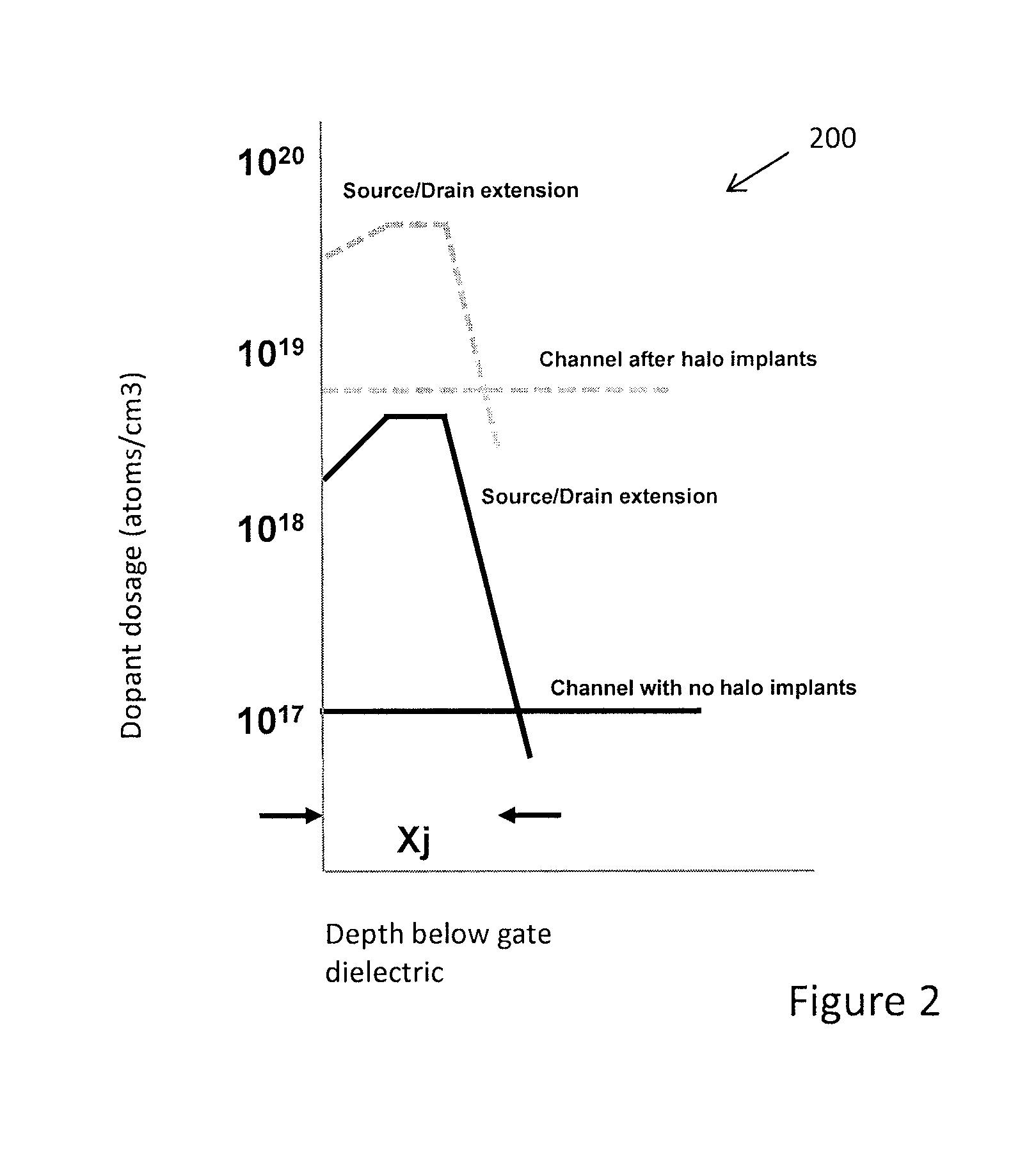
Unfortunately, traditional techniques for controlling channel spacing and reducing short channel effects can require source / drain extensions (typically formed by out-diffusion under gate spacers) or halo implants to reduce source / drain junction gradients.
Unfortunately, both conventional source / drain extensions and halo implants can cause contamination of a channel with unwanted dopants, reducing or destroying the advantages of the undoped channel or transistors with DDC structures.
The problem of channel dopant contamination can become even more acute when die supporting multiple transistor types or requiring multiple implants are implicated.
Multiple implants increase the likelihood of dopant diffusion into the channel, with each implant becoming a potential source of channel contamination.
In addition, each separate source / drain extension and halo implant process step can cause silicon erosion of the substrate layer due to a cleaning (ashing) step, and can risks damage to transistor gate dielectric corners due to lateral oxidation.
In “system on a chip,” microprocessor, or mixed signal processors, as well as many other advanced devices such as memory, FPGA, or analog / digital sensors, dozens of separate source / drain extensions and halo implants are often used in every die, with each implant process step introducing more dopant contaminants, slightly degrading the transistor gate structure, and increasing the risk of transistor failure.
Even simple time delays between source / drain extensions and halo implant process steps can cause increased exposure of the gate dielectric layers to oxidation that damages the gate dielectric.
While use of silicon nitride “L”-shaped spacers has been suggested to protect gate dielectrics from lateral oxidation “corner” attack during the multiple source / drain extensions and halo implant process steps, the space required to form L spacers typically reduces inter-transistor spacing, and complicates other processing steps such as growth or placement of tensile films or source / drain strain implants.

