Specimen box for electron microscope
a technology of electron microscope and specimen box, which is applied in the field of specimen boxes, can solve the problems of inability to observe specimen stimuli under the conventional electron microscope, inability to select specimens, invalidation of conventional electron microscope selection, etc., and achieve the effect of prolonging the in-situ observation time effectively
- Summary
- Abstract
- Description
- Claims
- Application Information
AI Technical Summary
Benefits of technology
Problems solved by technology
Method used
Image
Examples
example 1
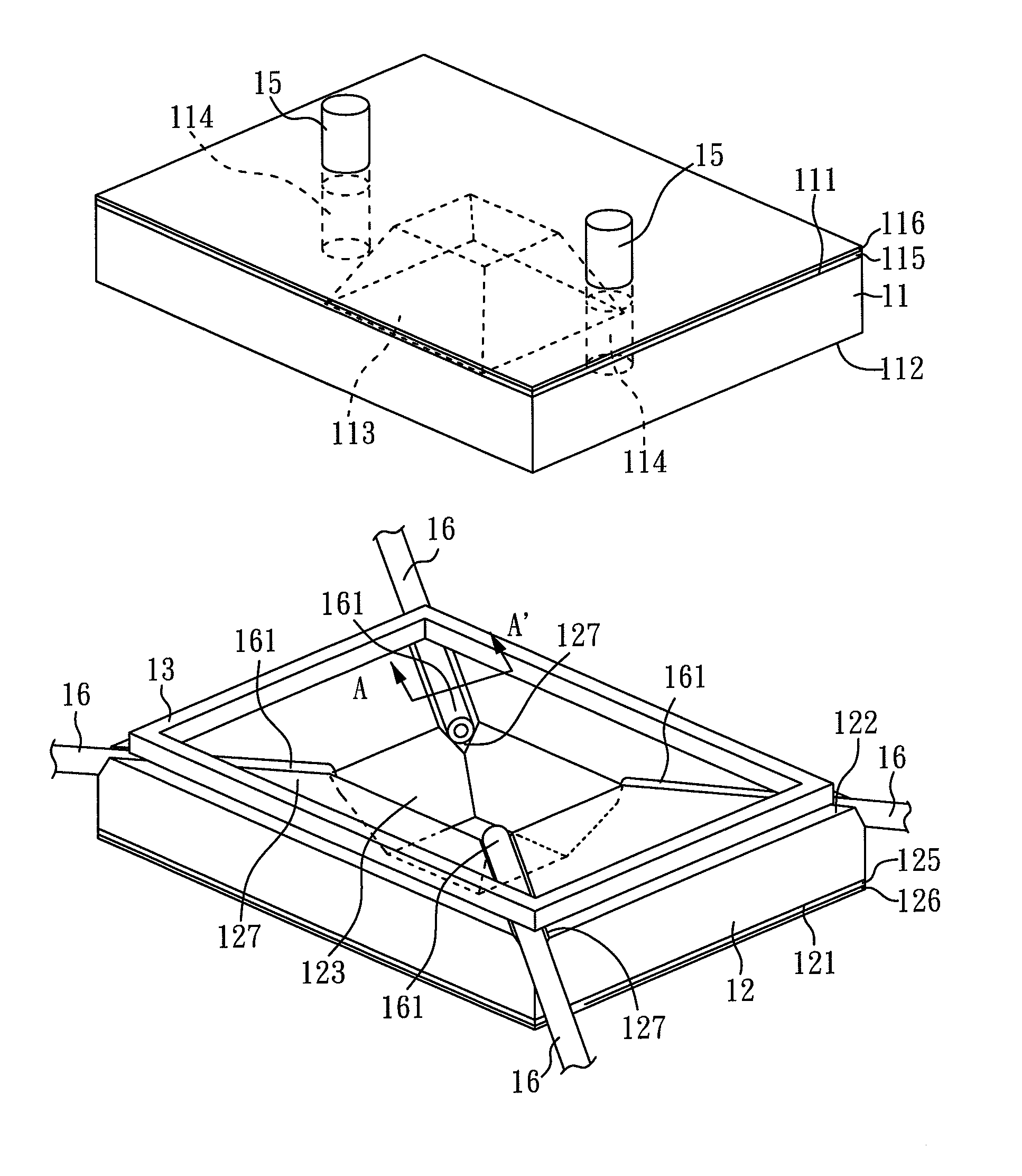
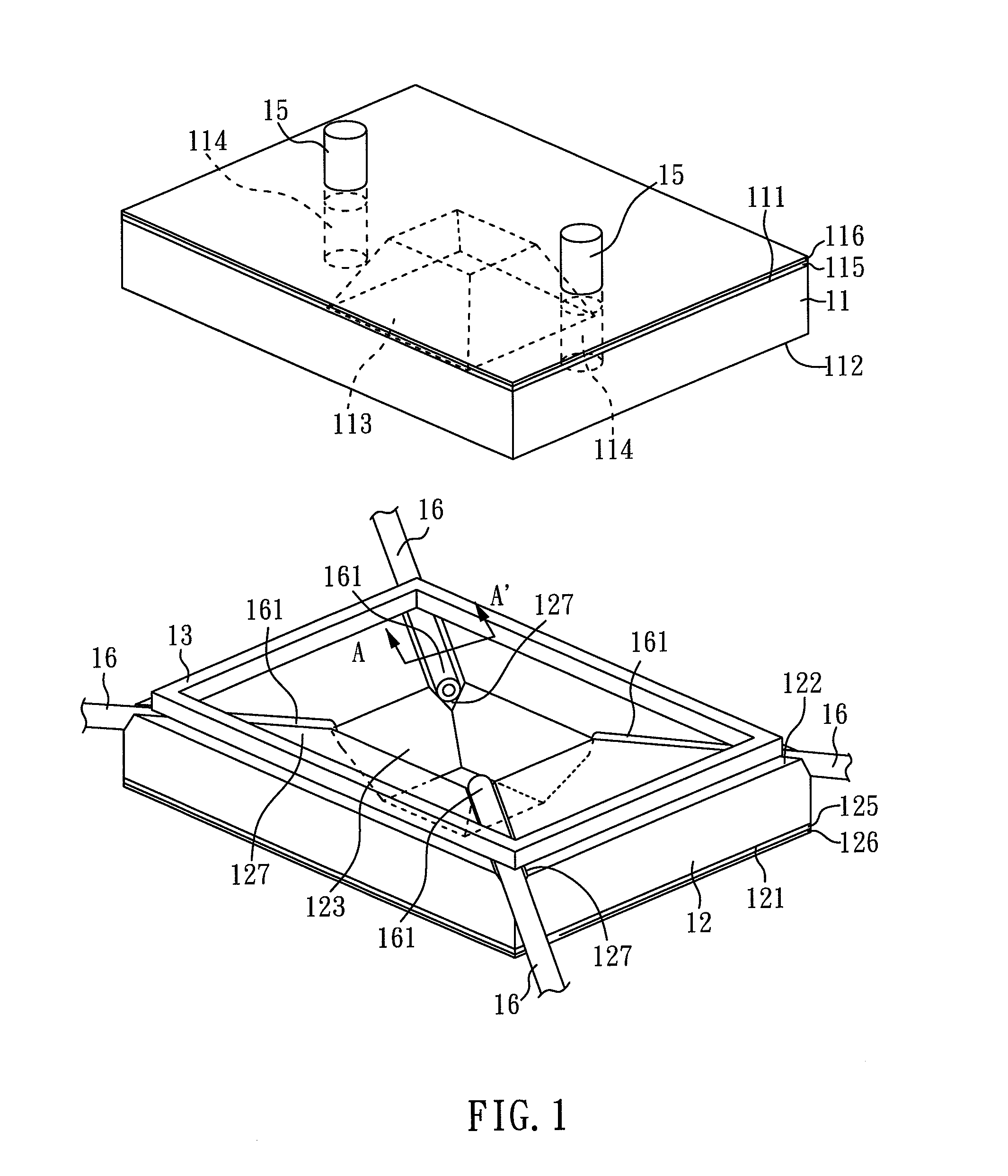
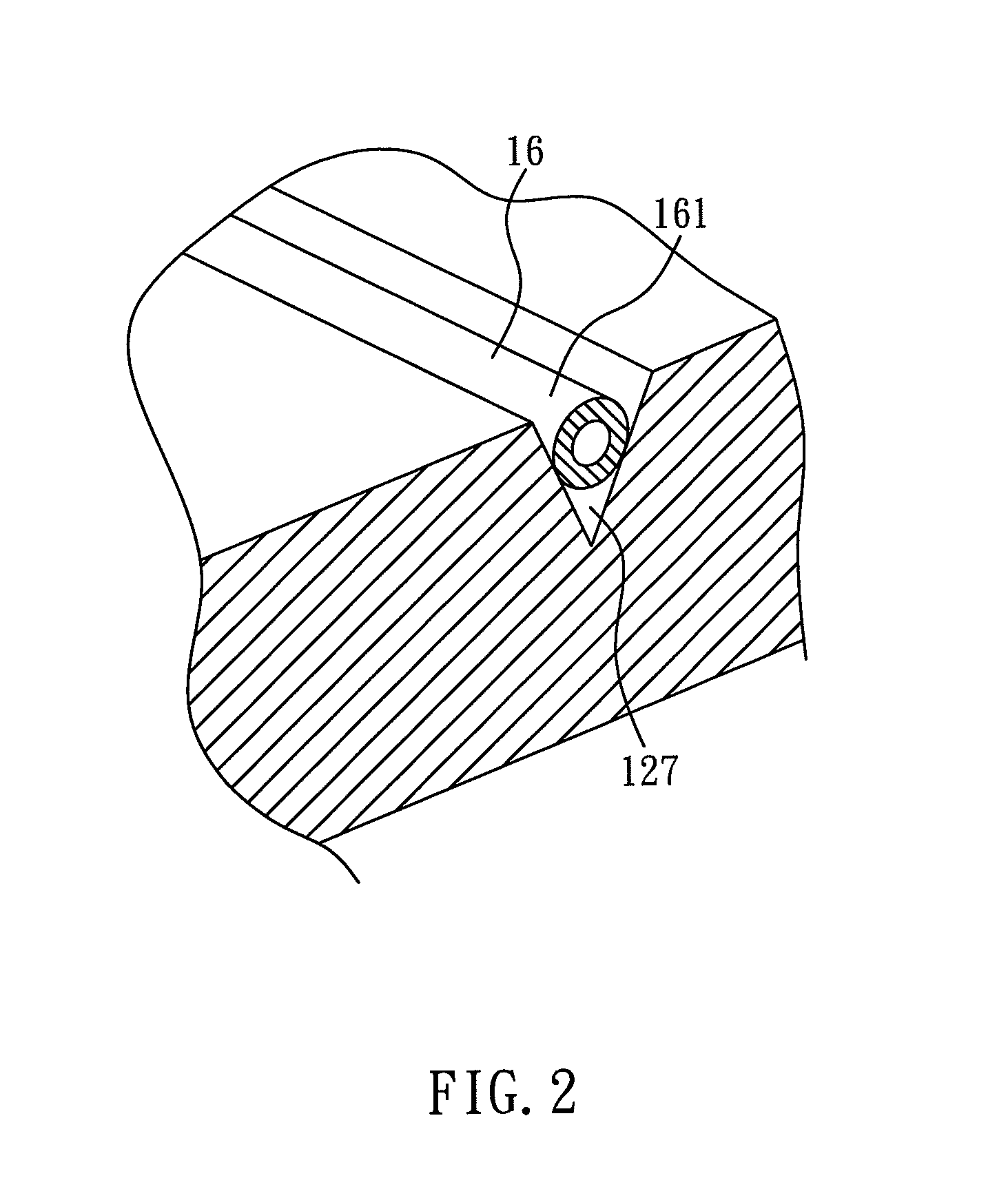
[0031]As showing in FIG. 1, FIG. 2, and FIG. 3, FIG. 1 a three-dimensional view showing the specimen box for electron microscope of the example 1; FIG. 2 is a three-dimensional view showing the photoelectric element of the specimen box for an electron microscope; and FIG. 3 is a three-dimensional view, which is shown along the A-A′ section line in FIG. 1, showing the specimen box for an electron microscope of the example 1. According toFIG. 1, FIG. 2, and FIG. 3, the specimen box of the present invention comprises: a first substrate 11, a second substrate 12, a metal adhesion layer 13, and four photoelectric elements 16. In the present example, the first substrate 11 and the second substrate 12 are (001) silicon substrate. The thickness of the first substrate 11 is 250 μm, and the thickness of the second substrate 12 is also 250 μm.
[0032]The first substrate 11 has a first surface 111, a second surface 112, a first concave 113, and two first through holes 114, in which the first conc...
example 2
[0045]FIG. 4 is a perspective view showing the specimen box for an electron microscope of the example 2. According to FIG. 4, the specimen box of the present example is roughly the same as example 1. The only difference is the disposition of the metal adhesion layer 13. In the present example, the metal adhesion layer 13 is disposed between the second surface 112 and the second protective layer 126. Four of the third concaves 117 are formed on the second surface 112 of the first substrate 11 by a dry etching process. The photoelectric element 16, which is disposed on the third concave 117, is an optical fiber, an electrode, or the combination thereof.[0046]The volume of the space (not shown) in the present example is 2 mm3. The height of the space (not shown) is 550 μm. In the present example, the volume of the space (not shown) is smaller than example 1, so the resolution is higher than example 1. Therefore, different volumes of the space (not shown) of the specimen box could be ch...
example 3
[0047]FIG. 5 is a perspective view showing the specimen box for an electron microscope of the example 3. According to the FIG. 5, the specimen box of present example is roughly the same as example 1. The only difference in the present example is the first thin film 115, the first protective layer 116, the second thin film 125, and the second protective layer 126 are only disposed on the first concave 113 and the second concave 123 to enhance the structure of the first concave 113 and the second concave 123. Therefore, the first thin film 115 and the second thin film 125 would not be cracked so as to avoid the specimen escaping from the space (not shown).
[0048]A fourth concave 127 is formed on the second surface 122 of the second substrate 12 by a wet etching process. The photoelectric element 16 is disposed on the fourth concave 127, in which the photoelectric element 16 is an optical fiber, an electrode, or a combination thereof.
[0049]In addition, the first through holes 114 and th...
PUM
 Abstract
Description
Claims
Application Information


