System and method for configurable digital communication

a digital communication and configurable technology, applied in static indicating devices, instruments, image memory management, etc., can solve problems such as limiting the performance potential of ground potential, limiting reference potential, and converting reference potential into signaling errors, so as to increase the complexity of products comprising, save the cost of producing many products, and save costs

Active Publication Date: 2013-04-09
NVIDIA CORP
View PDF167 Cites 21 Cited by
  • Summary
  • Abstract
  • Description
  • Claims
  • Application Information

AI Technical Summary

Benefits of technology

[0008]Embodiments of the present invention provide a system and method for digital communication with either differential or single-ended frame buffer memory, where the amount of frame buffer memory can be varied. And in contrast to prior art solutions, embodiments of the present invention provide these benefits without significantly increasing the cost or complexity of the interface.
[0010]In another embodiment of the present invention, the coupled device may be a detachable frame buffer memory. As such, an existing PCI-Express interface may be reconfigured to provide a differential interface for communication with frame buffer memory, thereby obviating the need for an additional interface. Thus, embodiments of the present invention represent significant cost savings without increasing the complexity of the products comprising and utilizing the interface.
[0011]In another embodiment of the present invention, an expansion interface device comprises a differential I / O interface, a plurality of memory devices, and a bus for coupling the differential I / O interface to the plurality of memory devices. The plurality of memory devices can be differential frame buffer memory. Alternatively, the plurality of memory devices can be single-ended frame buffer memory coupled to the differential I / O interface via a controller for converting the differential signal to a single-ended signal. Thus, embodiments of the present invention obviate the need to research, design, manufacture, and market a multitude of video cards with different amounts and types of frame buffer memory. As a result, the manufacturer can vary the amount of differential or single-ended frame buffer memory utilized by a single product, thereby saving the cost of producing many products without significantly increasing the complexity of the product.

Problems solved by technology

Despite being less expensive to integrate, there are downsides to single-ended signaling that limit its performance potential.
Also, differences between ground path and signal path length, coupled with the higher current in the ground path due to signal return-current sharing, can lead to ground potential variations throughout the system.
These variations in the reference potential then translate into signaling errors given that the signal potential does not similarly vary with the ground potential.
And given that the signal and ground paths do not run in the same proximity to one another, noise injected on the signal path is not similarly injected on the ground path, making single-ended signaling more susceptible to noise.
High signal voltages require higher transmission power, ultimately limiting transmission distance.
And even more importantly, the higher rise and fall times of the higher signal voltages limit interface speed and bandwidth.
Given these disadvantages, the computer industry is slowly moving toward differential signaling.
Moreover, the speed (e.g., 533 MHz for PCI-X 533) and additional hardware (e.g., almost twice as many pins used in the 64-bit PCI-X interfaces compared to the 32-bit PCI interfaces) used in the PCI-X interface makes it very costly to implement.
However, the transition to differential signaling will not occur immediately, thereby requiring video card manufacturers to implement backward compatibility with single-ended peripherals.
As such, it becomes extremely costly for a manufacturer to research, design, manufacture, and market a multitude of products to satisfy the demands of each market.

Method used


Image

  • System and method for configurable digital communication
  • System and method for configurable digital communication
  • System and method for configurable digital communication

Examples


Embodiment Construction

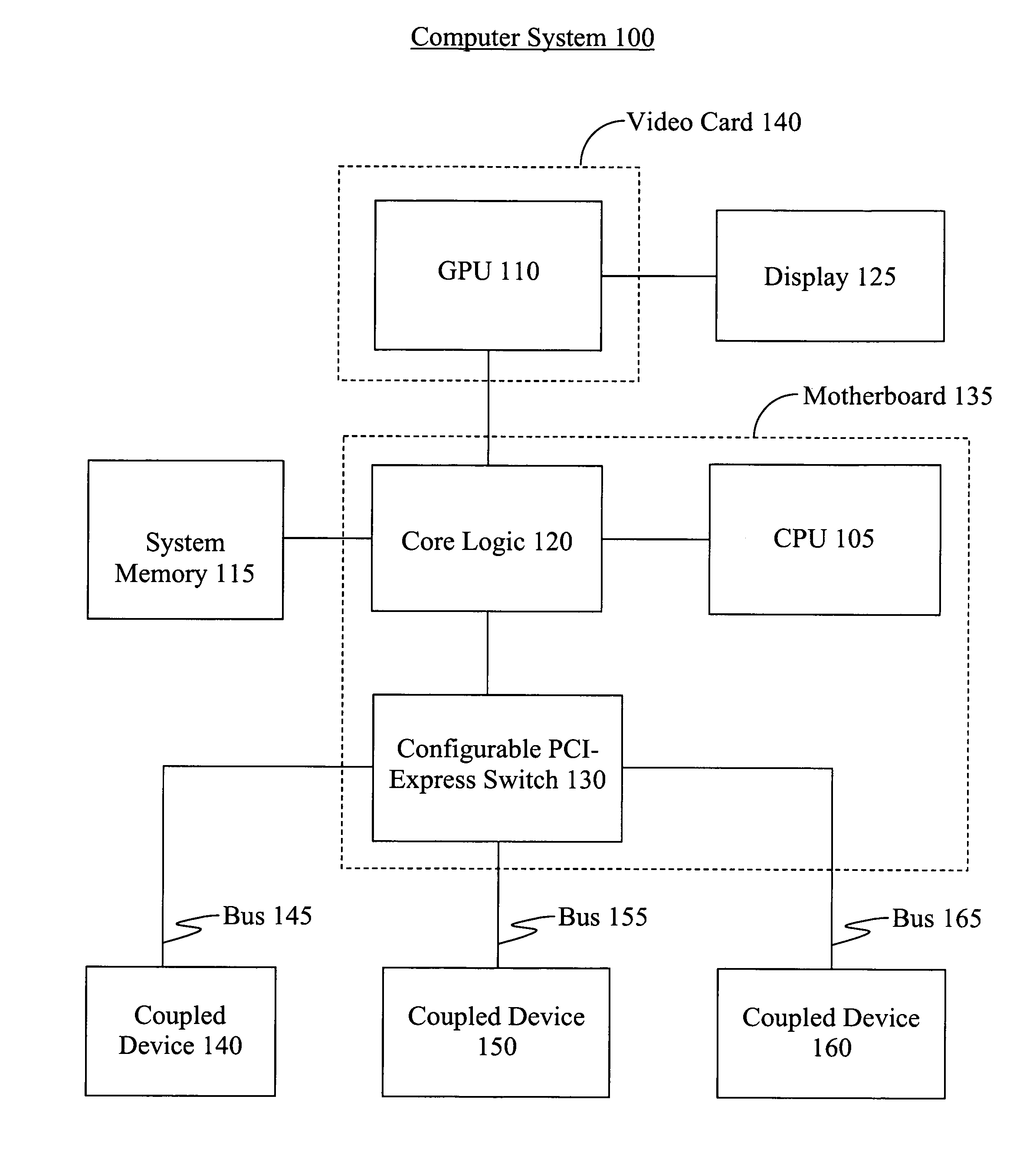
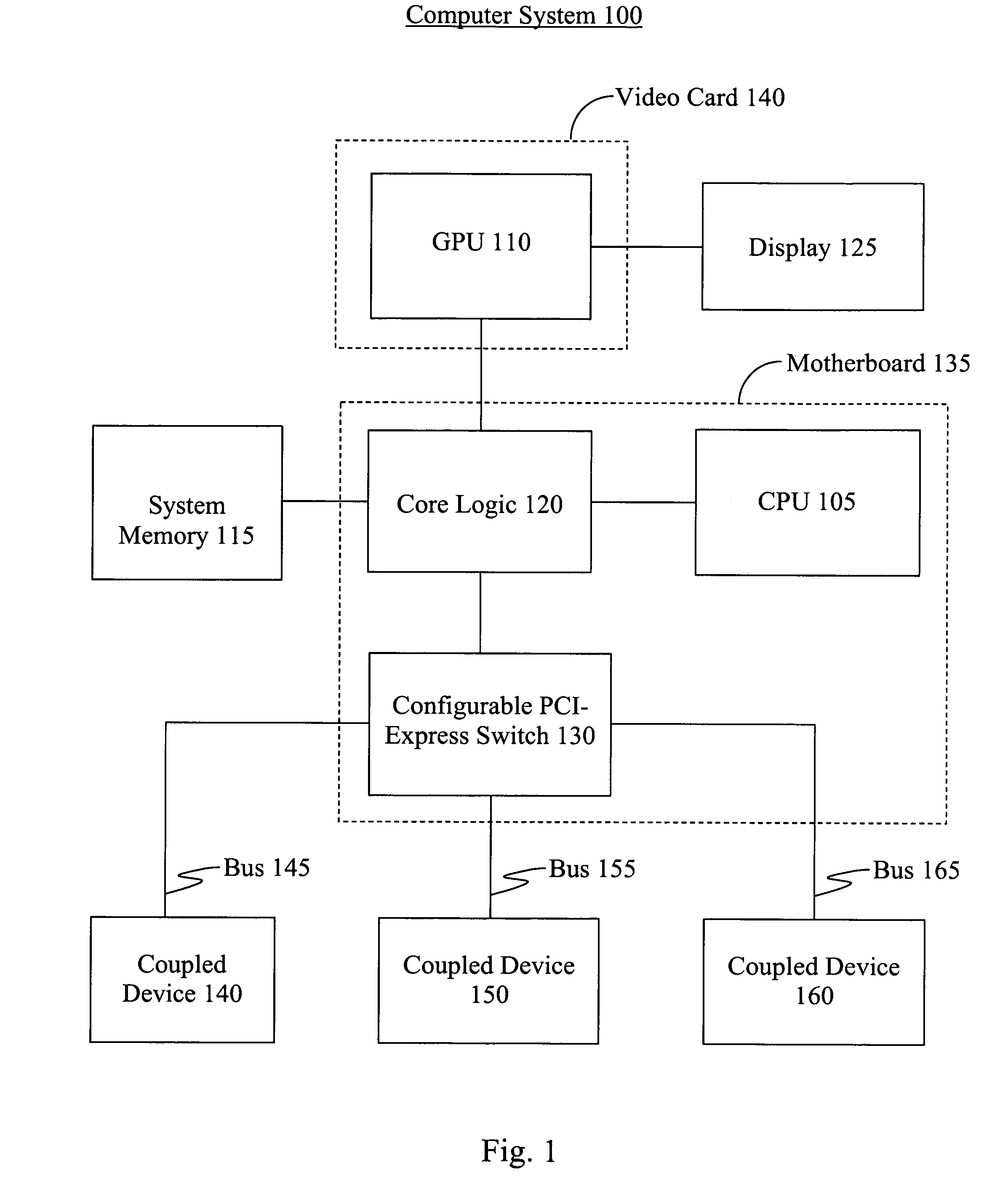
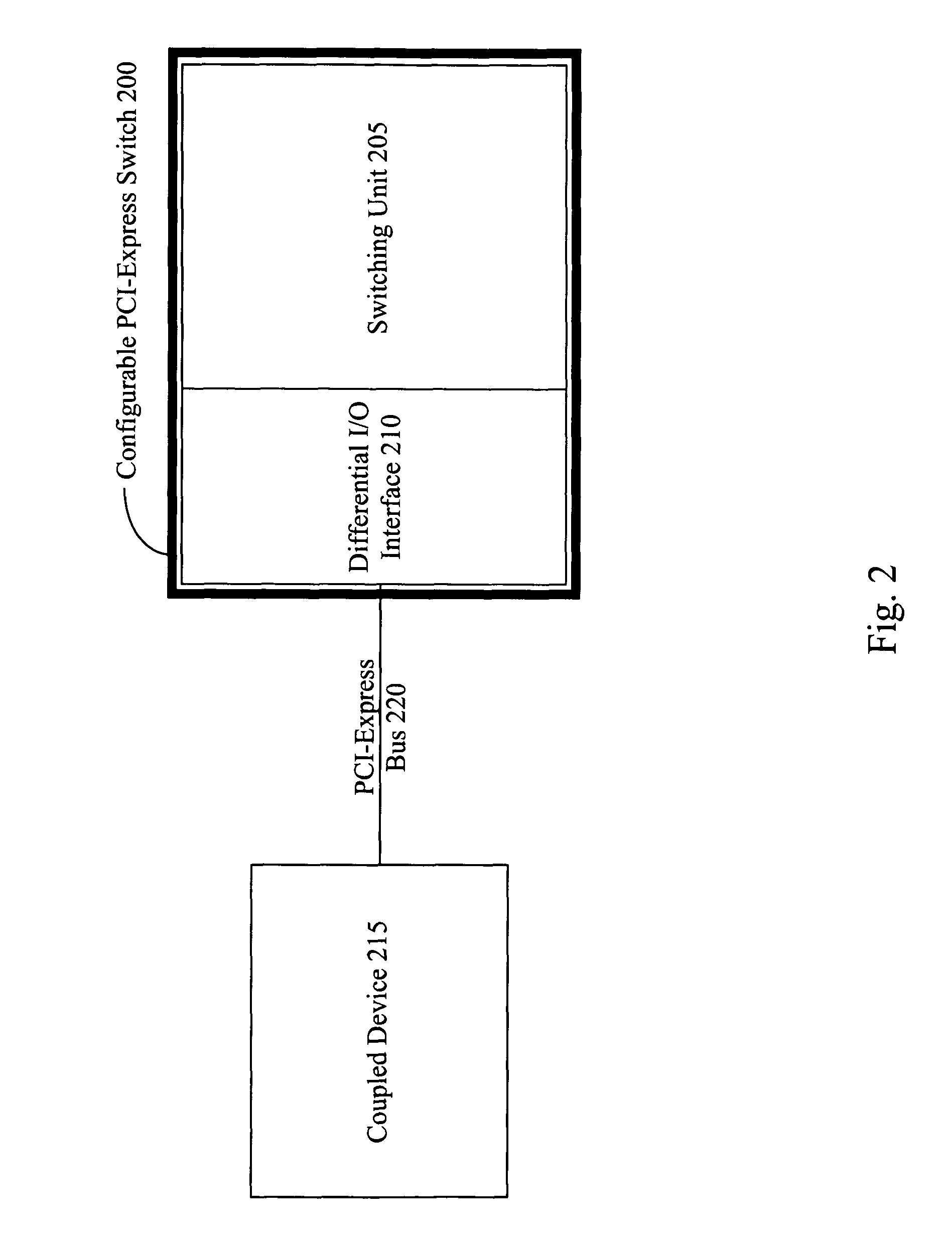
[0019]Reference will now be made in detail to the preferred embodiments of the present invention, examples of which are illustrated in the accompanying drawings. While the invention will be described in conjunction with the preferred embodiments, it will be understood that they are not intended to limit the invention to these embodiments. On the contrary, the invention is intended to cover alternatives, modifications, and equivalents, which may be included within the spirit and scope of the invention as defined by the appended claims. Furthermore, in the following detailed description of embodiments of the present invention, numerous specific details are set forth in order to provide a thorough understanding of the present invention. However, it will be recognized by one of ordinary skill in the art that the present invention may be practiced without these specific details. In other instances, well-known methods, procedures, components, and circuits have not been described in detail...


PUM


Abstract

The present invention pertains to a configurable PCI-Express switch. The configurable PCI-Express switch includes a differential I / O interface capable of being configured in a first configuration or a second configuration. In the first configuration, the differential I / O interface implements a PCI-Express interface with a coupled device. In the second configuration, the differential I / O interface implements a differential interface other than PCI-Express with the coupled device. The configurable PCI-Express switch also includes a switching unit capable of configuring the differential I / O interface in the first configuration or the second configuration.

Description

FIELD OF THE INVENTION[0001]The field of the present invention pertains to electronic integrated circuits, and more particularly to configurable PCI-Express switches.BACKGROUND OF THE INVENTION[0002]Until recently, computer systems have primarily utilized single-ended buses and interfaces. Single-ended signaling involves varying voltage with respect to a reference voltage, which is sometimes referred to as “ground,” to signal a logical “1” or “0.” When running multiple signals with respect to the same ground, single-ended signaling provides a cost-effective solution as it only requires one wire per signal.[0003]Despite being less expensive to integrate, there are downsides to single-ended signaling that limit its performance potential. For example, multiple signals sharing the same ground path can lead to crosstalk. Also, differences between ground path and signal path length, coupled with the higher current in the ground path due to signal return-current sharing, can lead to ground...

Claims


Application Information

Patent Timeline
Patent Type & Authority Patents(United States)
IPC IPC(8): G06F3/00
CPCG06F13/387
Inventor TAMASI, ANTHONY MICHAELWAGNER, BARRY A.MONTRYM, JOHN S.
Owner NVIDIA CORP
Why Eureka
Try Eureka