Semiconductor memory device having regular area and spare area

a memory device and semiconductor technology, applied in the field of semiconductor memory devices, can solve the problems of long trimming time, and achieve the effect of reducing the trimming time of the semiconductor memory devi

Inactive Publication Date: 2013-04-16
LONGITUDE SEMICON S A R L
View PDF14 Cites 0 Cited by
  • Summary
  • Abstract
  • Description
  • Claims
  • Application Information

AI Technical Summary

Benefits of technology

[0011]According to the present invention, when the number of addresses to be relieved is small, only one of a plurality of relief address storing area is used to store the relief address for relief of a defective cell, thereby reducing trimming time of the semiconductor memory device.

Problems solved by technology

In the initial stage of development of a processing technique, optimization is insufficient and therefore the defective cell tends to occur, so that it is necessary to previously mount a large number of fuse elements F. Accordingly, in the initial stage of the development, i.e., at the stage when a large number of fuse elements F are subjected to interruption, a long time is required for the trimming.

Method used


Image

  • Semiconductor memory device having regular area and spare area
  • Semiconductor memory device having regular area and spare area
  • Semiconductor memory device having regular area and spare area

Examples


first embodiment

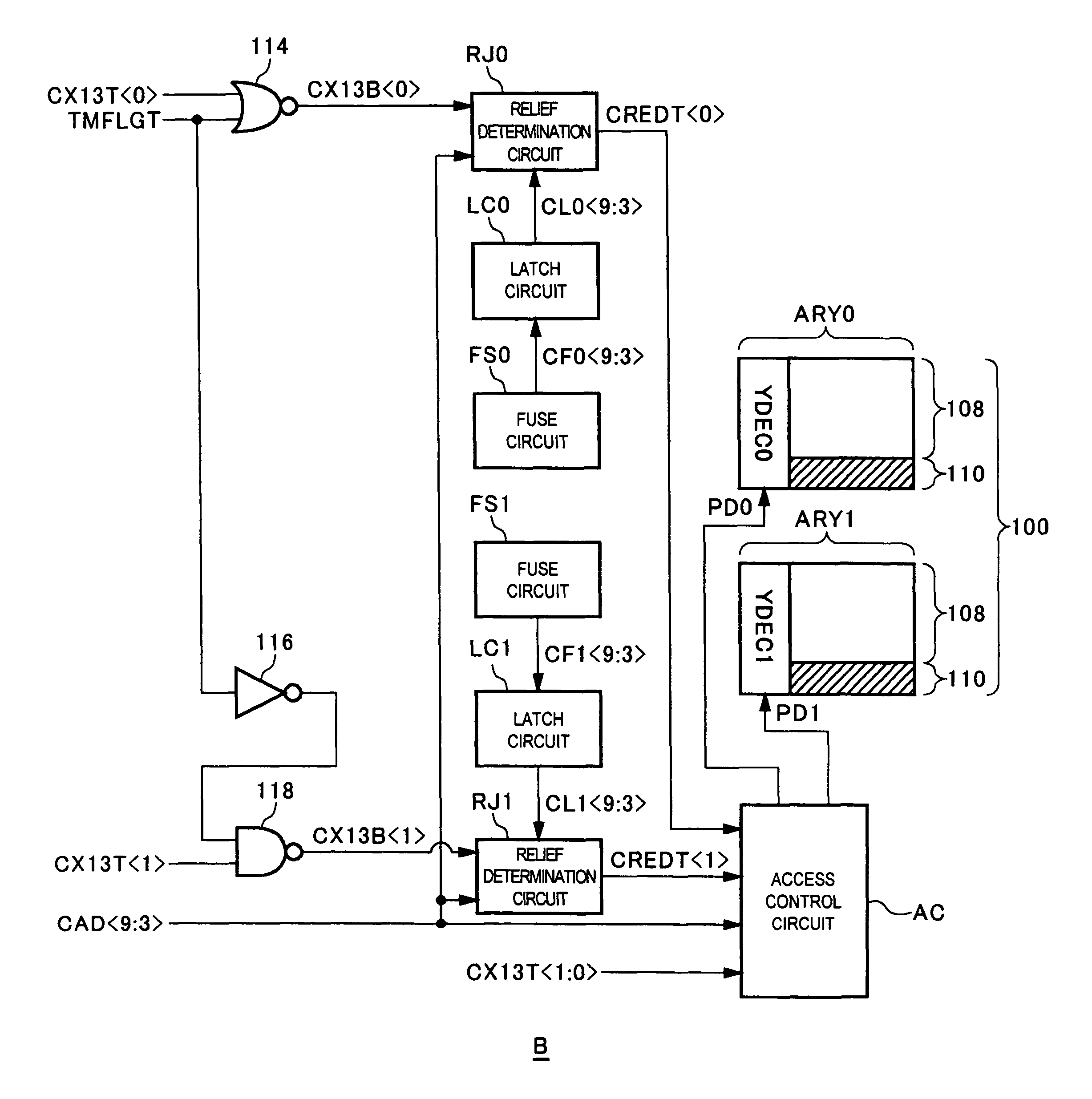
[0024]FIG. 1 is a peripheral circuit diagram of a bank B of a semiconductor memory device 10 according to a first embodiment of the present invention. A description will be given of a circuit configuration of the bank B first and then operation thereof. The circuit illustrated in FIG. 1 is housed in one bank B. A memory area 100 of the bank B is roughly divided into a lower address side memory array ARY0 (first memory area) and an upper address side memory array ARY1 (second memory area). In the present embodiment, it is assumed that the bank have an address width of 13 bits and that an address whose most significant bit (X=13) is 0 correspond to the memory array ARY0 and address whose most significant bit (X=13) is 1 correspond to the memory array ARY1.

[0025]The memory arrays ARY0 and ARY1 each include a regular area 108 and a spare area 110 and have, respectively, Y decoder YDEC0 and a Y decoder YDEC1 for selecting a column address. The Y decoders YDEC0 and YDEC1 are controlled by...

second embodiment

[0059]FIG. 7 is a peripheral circuit diagram of the bank B of the semiconductor memory device 10 according to a second embodiment of the present invention. The components designated by the same reference numerals as those in FIG. 1 have the same function as the components illustrated in FIG. 1. The bank B in the second embodiment controls the activation of the relief determination circuits RJ0 and RJ1 by means of the NOR circuit 114 and inverter 124.

[0060]Based on the circuit configuration described above, a concrete relief address control method will be described below.

[0061](1) In the Case Where the Number of Relief Addresses is More than a Predetermined Value

[0062]The lower-address side relief address is recorded in the fuse circuit FS0, and upper-address side relief address is recorded in the fuse circuit FS1. At this time, the TMFLGT is set to “L”.

[0063]1-1: When the Designation Address is Lower Address (CX13T0>=“H”, CX13T1>=“L”)

[0064]The relief determination circuit RJ0 is act...

third embodiment

[0079]FIG. 8 is a peripheral circuit diagram of the bank of the semiconductor memory device 10 according to a third embodiment of the present invention. The third embodiment relates to an access control method employed in the case where the relief addresses of two banks are collectively recorded in one fuse circuit FS0. The banks B0 and B1 each include a regular area 108 and a spare area 110. Further, the banks B0 and B1 each have an X-decoder (not illustrated) for selecting a row address. The X-decoder of the bank B0 is controlled by a pre-decode signal PD0 of an access control circuit AC0, and X-decoder of the bank B1 is controlled by a pre-decode signal PD1 of an access control circuit AC1.

[0080]Data of the relief address read out from the fuse circuit FS0 is supplied to the relief determination circuit RJ0. Data of the relief address read out from the fuse circuit FS1 is supplied to the relief determination circuit RJ1.

[0081]RBA0T is a two-bit signal indicating the most signific...


PUM


Abstract

Memory arrays ARY0 and ARY1 each include a regular area 108 and spare area 110. Fuse circuits FS0 and FS1 each store a relief address. Relief determination circuits RJ0 and RJ1 are provided so as to correspond to the fuse circuits FS0 and FS1, respectively. The relief determination circuits RJ0 and RJ1 each determine whether a designation address is the relief address or not. An access control circuit AC specifies an access destination from the memory array ARY0 or ARY1 according to the determination results. When it is determined by the relief determination circuit RJ0 that the designation address corresponds to the relief address, the access control circuit AC selects one of the memory arrays ARY0 and ARY1 according to CX13T<1:0> and selects the spare area 110 included in the selected memory array ARY as an access target.

Description

BACKGROUND OF THE INVENTION[0001]1. Field of the Invention[0002]The present invention relates to a semiconductor memory device and, more particularly, to a semiconductor memory device having an access control circuit for accessing a relief address.[0003]2. Description of Related Art[0004]In a semiconductor memory device such as a DRAM (Dynamic Random Access Memory), the number of memory cells (hereinafter referred to as “defective cell”) that do not operate properly is increased with an increase in a memory capacity. To cope with this problem, spare memory cells called “redundant cells” are prepared in such a semiconductor memory device, and the defective cell is replaced by the redundant cell so as to relieve the memory address of the defective cell. Hereinafter, the address of the defective cell is referred to as “relief address”. Detection of the defective cell and replacement of the detected defective cell by the redundant cell are performed in a wafer state of the semiconductor...

Claims


Application Information

Patent Timeline
Patent Type & Authority Patents(United States)
IPC IPC(8): G11C8/12
CPCG11C8/06G11C11/408G11C8/12
Inventor TAHARA, KAORU
Owner LONGITUDE SEMICON S A R L
Why Eureka
Try Eureka