Nitride semiconductor laser diode

a laser diode and semiconductor technology, applied in the direction of lasers, semiconductor devices, semiconductor lasers, etc., can solve the problem that the laser oscillation efficiency is not necessarily excellent, and achieve the effect of reducing the threshold current and improving the laser oscillation efficiency

Inactive Publication Date: 2013-04-30
ROHM CO LTD
View PDF9 Cites 0 Cited by
  • Summary
  • Abstract
  • Description
  • Claims
  • Application Information

AI Technical Summary

Benefits of technology

[0009]An object of the present invention is to provide a nitride semiconductor laser diode capable of improving laser oscillation efficiency and reducing a threshold current.

Problems solved by technology

Therefore, the efficiency of laser oscillation is not necessarily excellent but must be improved for reducing the threshold current.

Method used


Image

  • Nitride semiconductor laser diode
  • Nitride semiconductor laser diode
  • Nitride semiconductor laser diode

Examples


Embodiment Construction

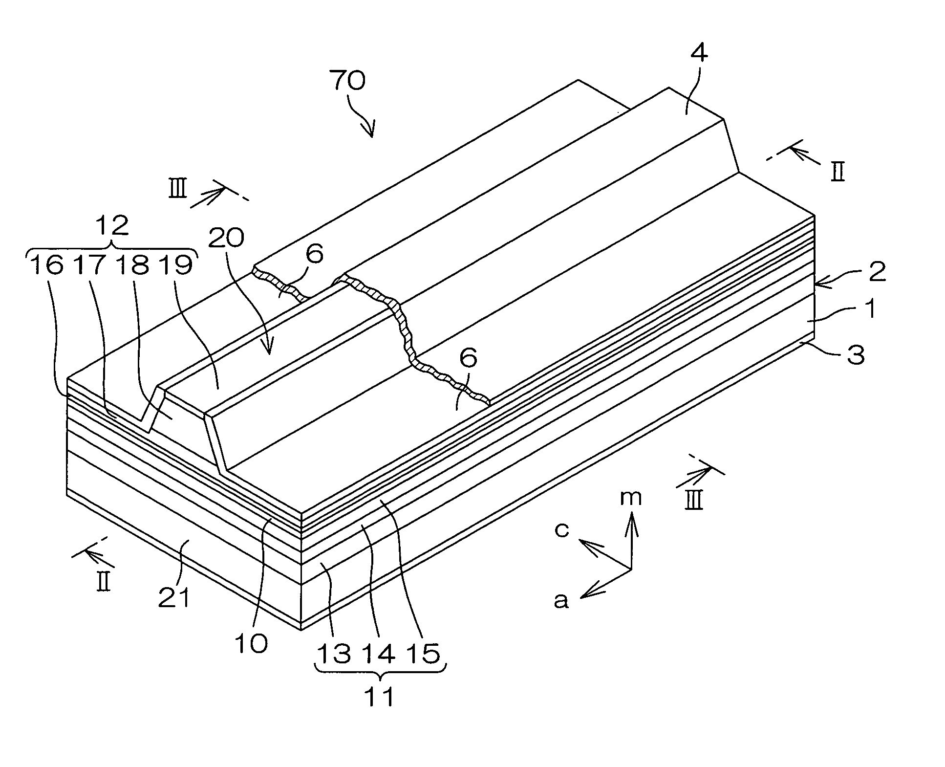
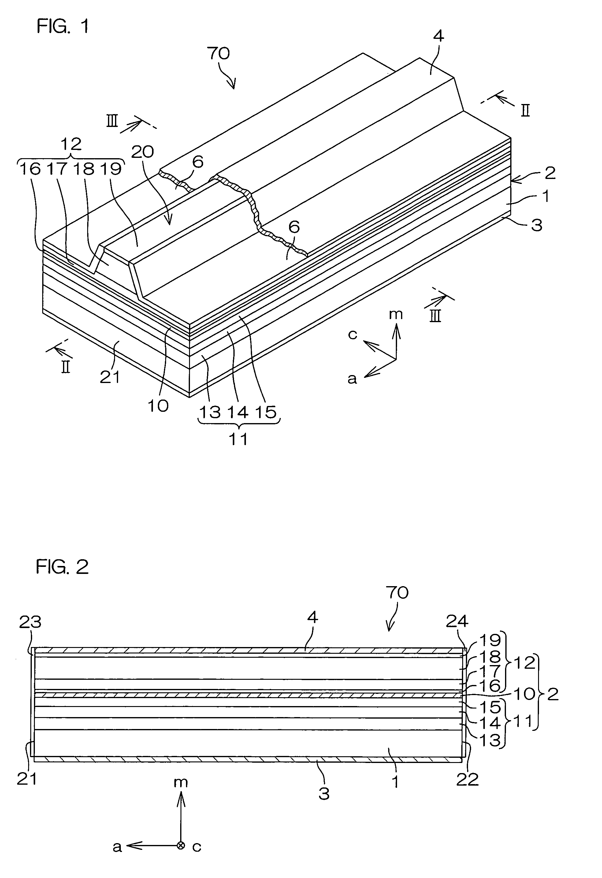
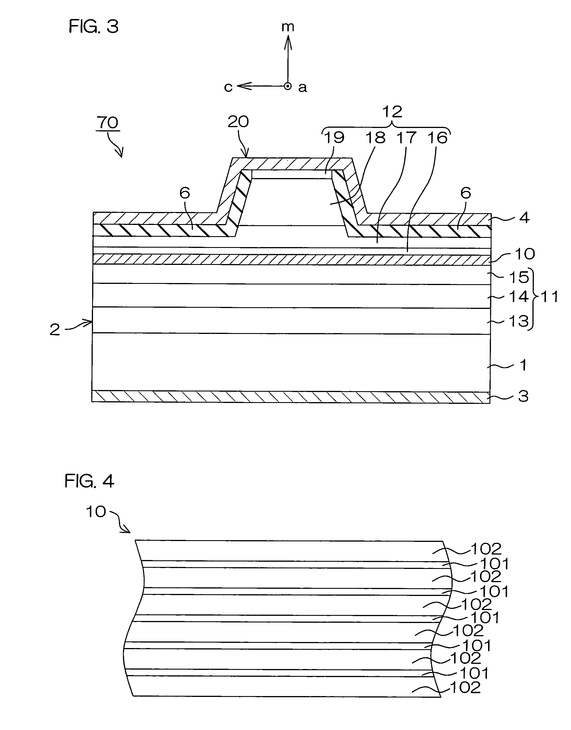
[0019]A nitride semiconductor laser diode according to an embodiment of the present invention has a quantum well layer consisting of a mixed crystal of AlxInyGa1-x-yN (x≧0.5, y≧0 and 1−x−y≦0.5) in a group III nitride semiconductor multilayer structure having a major growth surface defined by a nonpolar plane (an m-plane or an a-plane), with a cavity direction is set perpendicular to a c-axis (preferably, parallel to the major growth surface and perpendicular to the c-axis).

[0020]No report has heretofore been made as to a prototype example of a nitride semiconductor laser diode including a quantum well layer made of a group III nitride semiconductor such as AlGaN, AlInGaN or AlInN having a composition containing Al and operating with a wavelength of not more than 365 nm.

[0021]The inventor of the present invention has manufactured a prototype semiconductor laser diode having a multiple quantum well layers including a quantum well layer comprising of a mixed crystal of AlxInyGa1-x-yN (...


PUM


Abstract

A nitride semiconductor laser diode has a quantum well layer consisting of a mixed crystal of Alx1Iny1Ga1-x1-y1N (x1≧0.5, y1≧0 and 1−x1−y1≦0.5) in a group III nitride semiconductor multilayer structure having a major growth surface defined by a nonpolar plane. A cavity direction of the laser diode is perpendicular to a c-axis. The major growth surface of the group III nitride semiconductor multilayer structure may be defined by an m-plane. In this case, the cavity direction may be along an a-axis.

Description

BACKGROUND OF THE INVENTION[0001]1. Field of the Invention[0002]The present invention relates to a nitride semiconductor laser diode including a semiconductor multilayer structure made of group III nitride semiconductors.[0003]2. Description of Related Art[0004]Group III-V semiconductors employing nitrogen as a group V element are called “group III nitride semiconductors”, and typical examples thereof include aluminum nitride (AlN), gallium nitride (GaN) and indium nitride (InN), which can be generally expressed as AlXInYGa1-X-YN (0≦X≦1, 0≦Y≦1 and 0≦X+Y≦1).[0005]Short wavelength laser sources such as blue and green laser sources are increasingly employed in the fields of high-density recording in optical disks represented by a DVD, image processing, medical instruments, measuring instruments and the like. Such a short wavelength laser source is constituted of a laser diode employing GaN semiconductors, for example.[0006]A GaN semiconductor laser diode is manufactured by growing grou...

Claims


Application Information

Patent Timeline
Patent Type & Authority Patents(United States)
IPC IPC(8): H01S3/04
CPCB82Y20/00H01S5/34333H01S5/0287H01S5/2009H01S5/22H01S5/2201H01S5/3063H01S5/3202H01S2302/00H01S5/32025
Inventor KUBOTA, MASASHI
Owner ROHM CO LTD
Why Eureka
Try Eureka