
Reconfigurable engineering change order base cell

a technology of engineering change order and base cell, applied in the direction of logic circuits characterised by logic functions, cad circuit design, pulse technique, etc., can solve the problems of increasing revenue loss, reducing market window access, and difficult to find an ideal distribution of spare cells

Active Publication Date: 2013-05-21
NXP USA INC
View PDF6 Cites 31 Cited by
  • Summary
  • Abstract
  • Description
  • Claims
  • Application Information

AI Technical Summary

Benefits of technology

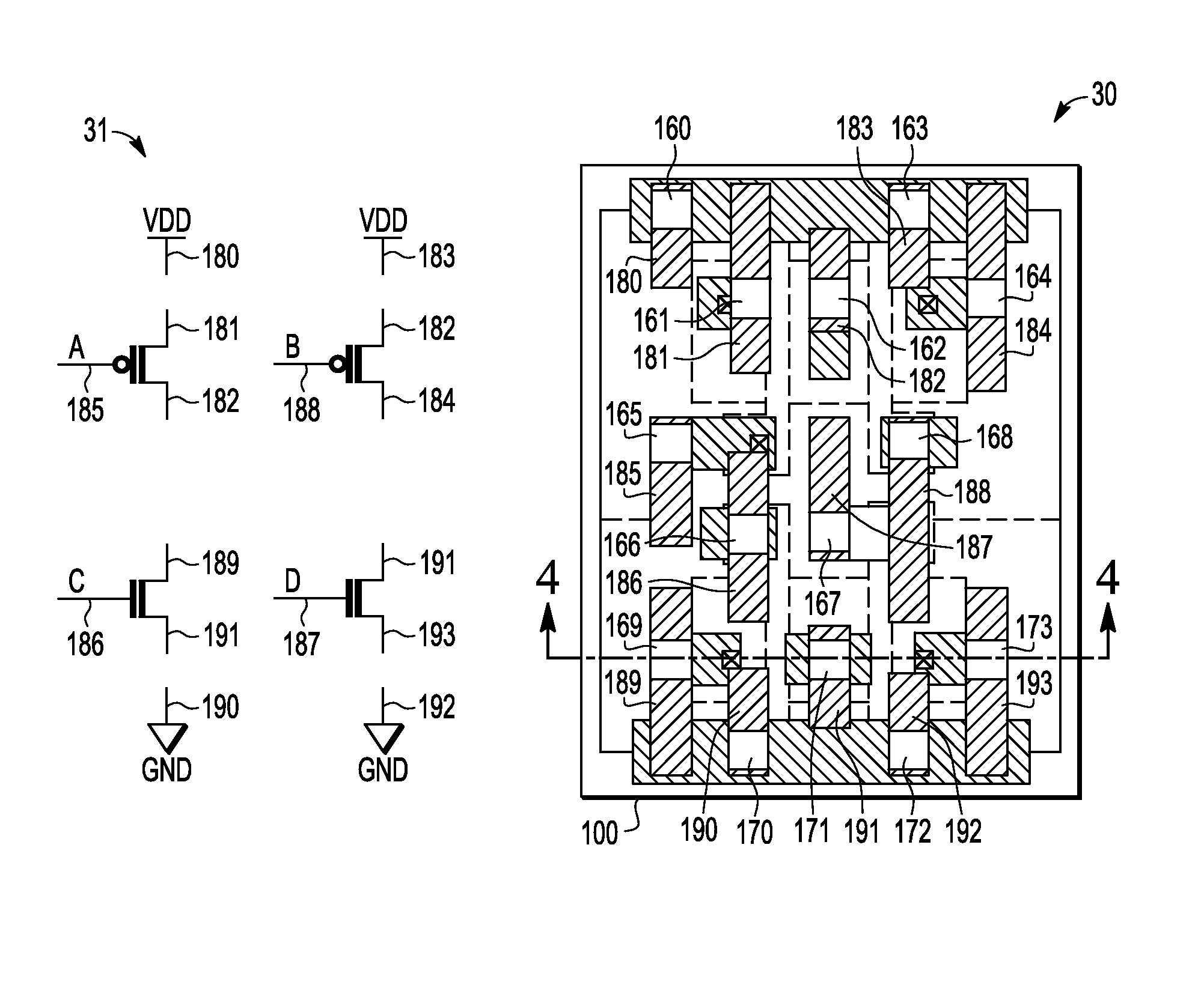
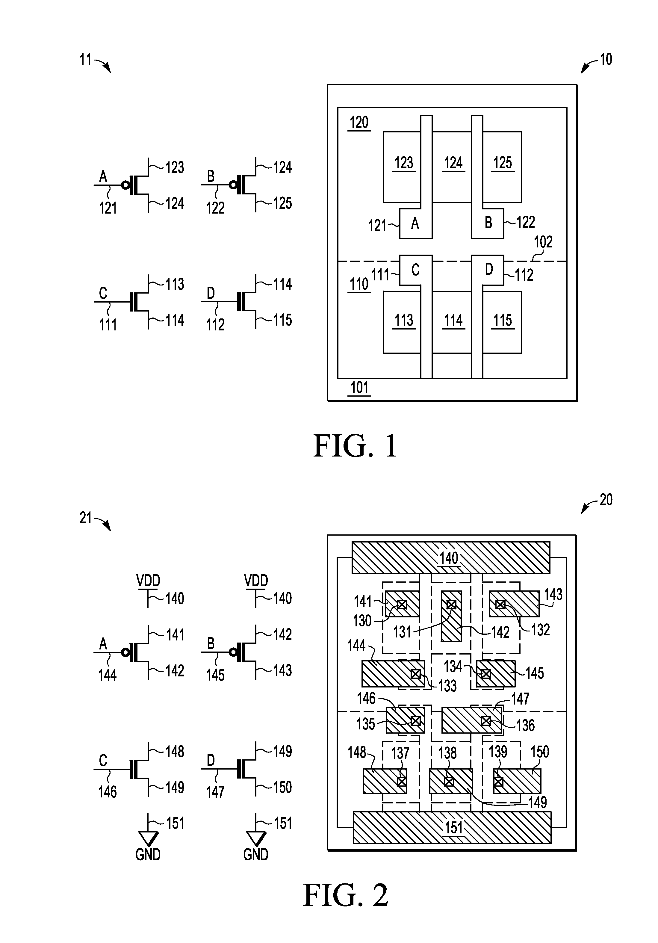
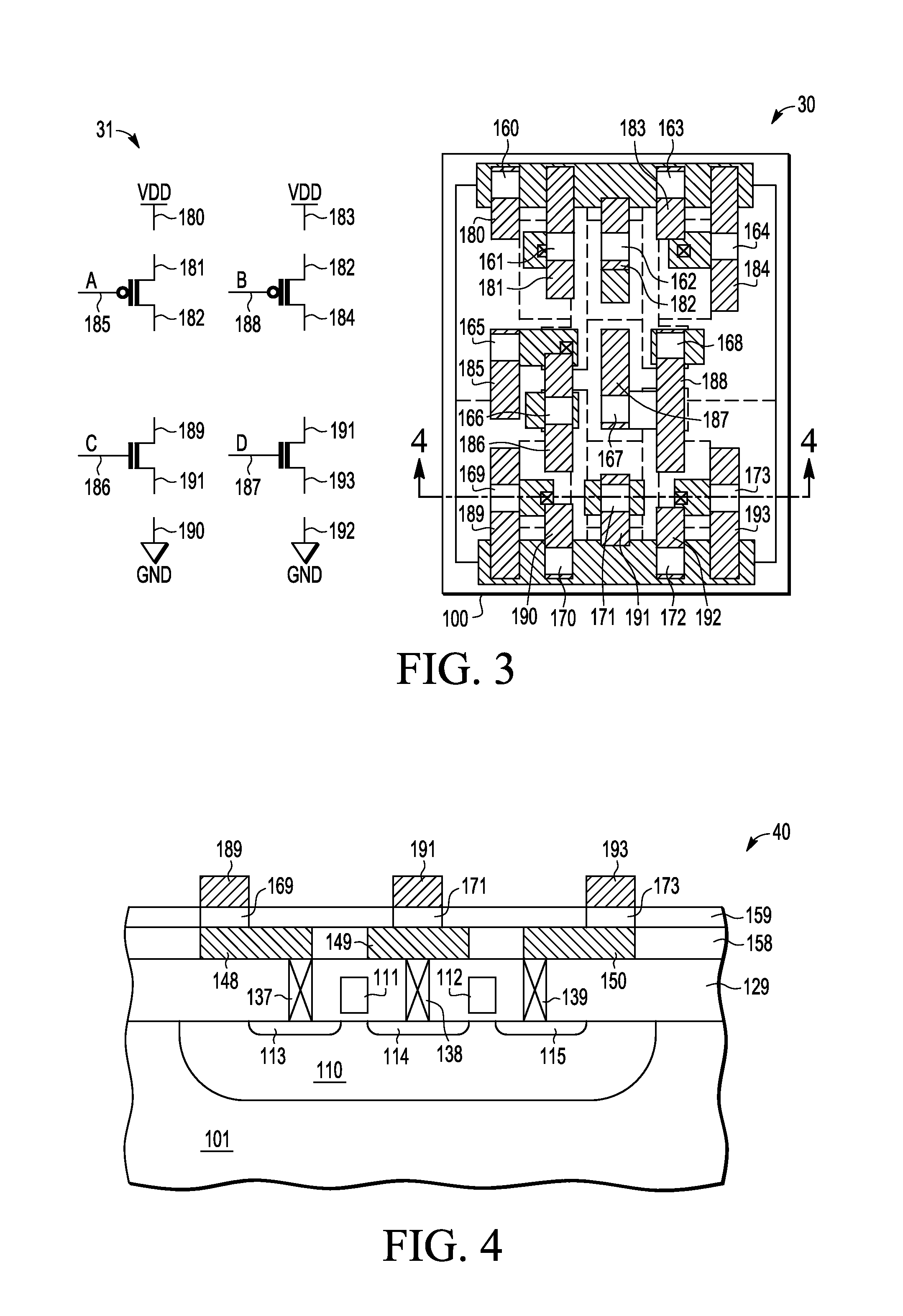
The present invention relates to integrated circuit design and proposes a method for managing changes to the design using a base cell approach. This allows for easier revision management and reduces the time and cost associated with redesign. The invention provides a reconfigurable ECO base cell that includes a plurality of transistors and reference voltage terminals that can be connected together in the conductors above the second metal layer to provide a variety of different circuit configurations. This allows for flexibility in the logic insertion process and reduces the need for long routing wires with increased propagation delay. The invention also includes a circuit schematic diagram for each of the base cell configurations and a process flow for implementing a design change using the reconfigurable ECO base cell. The technical effects of the invention include improved efficiency and flexibility in integrated circuit design and reduced redesign costs and time.

Problems solved by technology

As design complexity and density increase, post silicon debugging and design correction can extend the design cycle, thereby reducing market window access and increasing revenue loss.
However, it is difficult to find an ideal distribution of spare cells since a poorly placed spare cell would require long routing wires with increased propagation delay, and a poor selection of cell types would require more cells to fix the same error.
To provide flexibility in the logic insertion process, programmable base cells have been proposed which are programmed at the contact and first metal layer and above to provide the required logic functionality, but such base cells have limited flexibility and associated performance limitations and costs.

Method used


Image

  • Reconfigurable engineering change order base cell
  • Reconfigurable engineering change order base cell
  • Reconfigurable engineering change order base cell

Examples


Embodiment Construction

[0023]A reconfigurable ECO base cell and associated design methodology are provided in which separated pull-up and pull-down networks are provided in a base cell which has a predefined substrate design and fixed conductor stack up to the second metal layer, and which may be programmed to provide a variety of different circuit configurations using only the metal and via layers above the second metal layer, thereby reducing the redesign cost and time. In selected embodiments, the reconfigurable ECO base cell includes a plurality of transistors (e.g., NMOS and PMOS transistors) and a plurality of reference voltage terminals (e.g., VDD and VSS) that are implemented between the substrate and second metal layers as electrically separate elements, and that may be connected together in the conductors above the second metal layer to provide a desired circuit functionality during the ECO redesign process. In other embodiments, the reconfigurable ECO base cell includes a plurality of transisto...


PUM


Abstract

An integrated circuit ECO base cell module is formed with PMOS and NMOS gate electrode structures and power supply lines that are electrically separated from one another up to the second metal (M2) layer in a fixed circuit structure that may be reconfigured with one or more conductor elements formed above the M2 layer to form a predetermined circuit function.

Description

BACKGROUND OF THE INVENTION[0001]1. Field of the Invention[0002]The present invention is directed in general to integrated circuit design. In one aspect, the present invention relates to design revision management using a base cell to implement Engineering Change Orders (ECOs).[0003]2. Description of the Related Art[0004]As design complexity and density increase, post silicon debugging and design correction can extend the design cycle, thereby reducing market window access and increasing revenue loss. In chip design, ECO is the process of inserting a logic change directly into the netlist after it has already been processed by an automatic tool, typically by inserting spare logic cells. However, it is difficult to find an ideal distribution of spare cells since a poorly placed spare cell would require long routing wires with increased propagation delay, and a poor selection of cell types would require more cells to fix the same error. To provide flexibility in the logic insertion pr...

Claims


Application Information

Patent Timeline
IPC IPC(8): H01L25/00H01L27/088H03K19/094H03K19/20
CPCG06F17/5068H01L27/0207H01L27/092G06F30/39
Inventor YANG, JIANANHUTCHINSON, DARRIN L.JAMISON, STEPHEN G.
Owner NXP USA INC
Learn More