Multilevel memory bus system for solid-state mass storage

a memory bus and multi-level technology, applied in the field of memory buses, can solve the problems of affecting the performance of memory bus designs, difficult to perform the memory capacity of these memory subsystems, and unable to adapt to such changes

Inactive Publication Date: 2013-05-21
BITMICRO LLC
View PDF3 Cites 63 Cited by
  • Summary
  • Abstract
  • Description
  • Claims
  • Application Information

AI Technical Summary

Problems solved by technology

Increasing the memory capacity of these memory subsystems is difficult to perform without also negatively impacting the memory performance of these memory subsystems, the integrity of data transferred through the memory bus of these mass storage devices, or both.
In addition, semiconductor technology continues to improve, and thus change, rendering known memory bus designs not readily adaptable to such change.

Method used


Image

  • Multilevel memory bus system for solid-state mass storage
  • Multilevel memory bus system for solid-state mass storage
  • Multilevel memory bus system for solid-state mass storage

Examples


Embodiment Construction

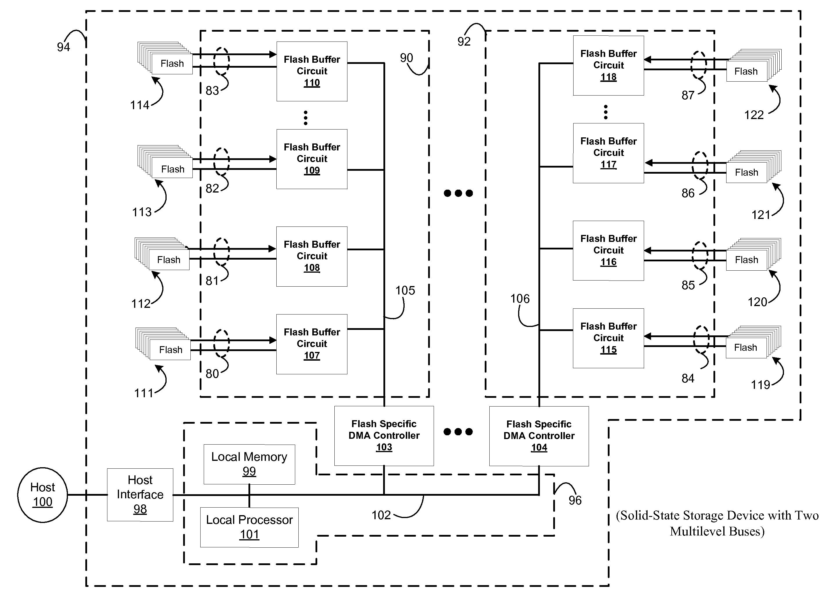
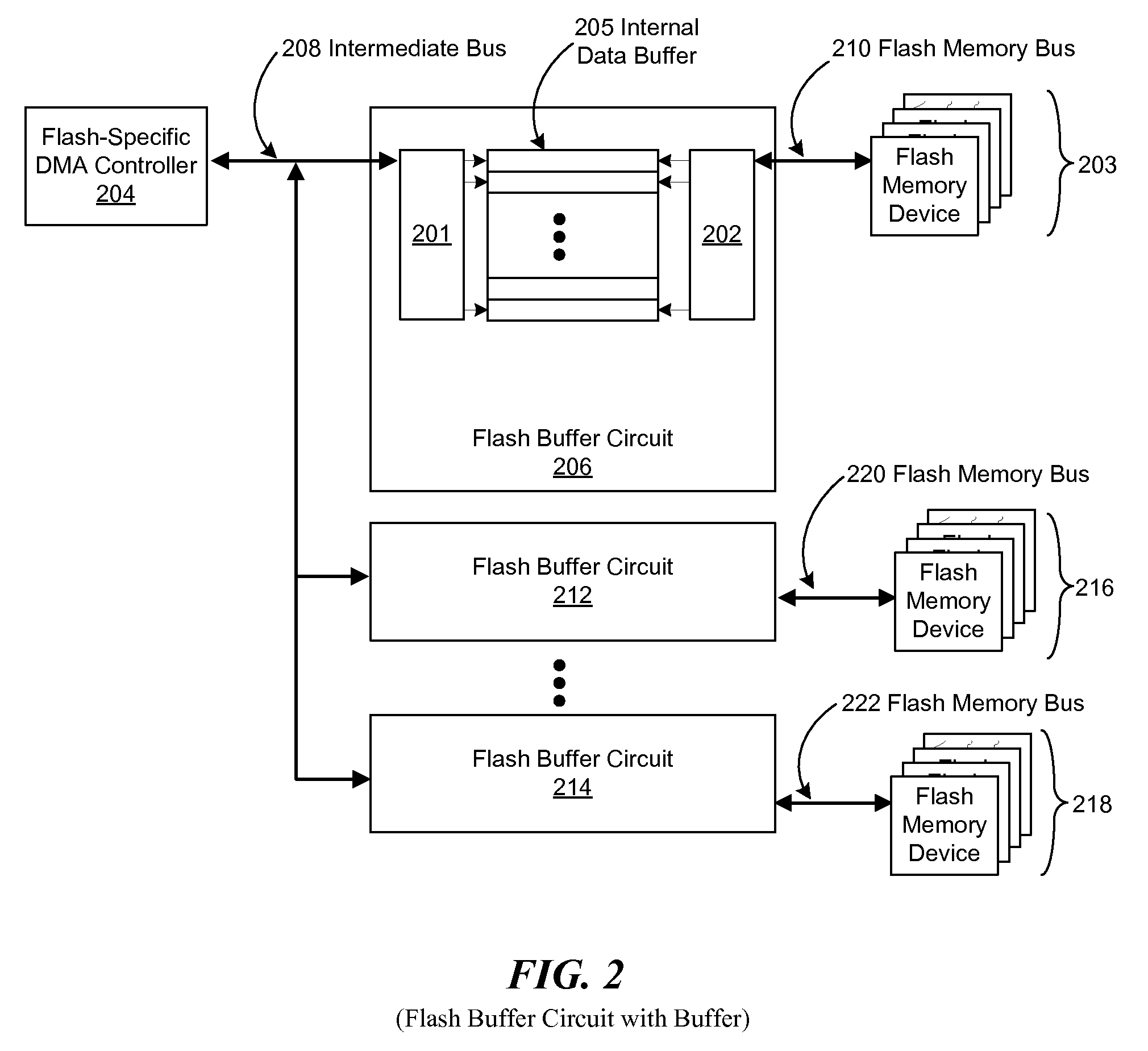
[0020]In the following detailed description, for purposes of explanation, numerous specific details are set forth to provide a thorough understanding of the various embodiments of the present invention. Those of ordinary skill in the art will realize that these various embodiments of the present invention are illustrative only and are not intended to be limiting in any way. Other embodiments of the present invention will readily suggest themselves to such skilled persons having the benefit of this disclosure.

[0021]In addition, for clarity purposes, not all of the routine features of the embodiments described herein are shown or described. One of ordinary skill in the art would readily appreciate that in the development of any such actual implementation, numerous implementation-specific decisions may be required to achieve specific design objectives. These design objectives will vary from one implementation to another and from one developer to another. Moreover, it will be appreciate...


PUM


Abstract

The present invention relates to a multilevel memory bus system for transferring information between at least one DMA controller and at least one solid-state semiconductor memory device, such as NAND flash memory devices or the like. This multilevel memory bus system includes at least one DMA controller coupled to an intermediate bus; a flash memory bus; and a flash buffer circuit between the intermediate bus and the flash memory bus. This multilevel memory bus system may be disposed to support: an n-bit wide bus width, such as nibble-wide or byte-wide bus widths; a selectable data sampling rate, such as a single or double sampling rate, on the intermediate bus; a configurable bus data rate, such as a single, double, quad, or octal data sampling rate; CRC protection; an exclusive busy mechanism; dedicated busy lines; or any combination of these.

Description

CROSS-REFERENCE(S) TO RELATED APPLICATIONS[0001]This application claims the benefit of United States Provisional application, entitled “Multilevel Memory Bus System for Solid-State Mass Storage”, having filing date of 7 Sep. 2009 and Ser. No. 61 / 240,246, which is hereby incorporated by reference as if fully set forth herein.BACKGROUND[0002](1) Technical Field[0003]The present invention relates to memory buses that can be used with computing devices that use solid-state mass storage, such as mass storage devices that use semiconductor memory devices as their respective mass storage memory store, named “solid-state mass storage devices”, and with computing devices that employ a solid-state memory subsystem.[0004](2) Description of the Related Art[0005]Unlike hard disk drives, solid-state storage devices are disposed with a solid-state memory subsystems comprising of a plurality of semiconductor memory devices that have addressable memory cells. Increasing the memory capacity of these ...

Claims


Application Information

Patent Timeline
Patent Type & Authority Patents(United States)
IPC IPC(8): G06F13/28G06F9/44G06F13/36
CPCG06F12/00G06F13/1657G06F12/0246G06F13/36G06F13/1673G06F13/1684
Inventor BRUCE, RICARDO H.VILLAPANA, ELSBETH LAUREN T.BAYLON, JOEL A.
Owner BITMICRO LLC
Why Eureka
Try Eureka