Methods of forming semiconductor trench and forming dual trenches, and structure for isolating devices

a technology of semiconductor trenches and isolation structures, applied in the direction of semiconductor/solid-state device manufacturing, basic electric elements, electric apparatus, etc., can solve the problems of increasing the difficulty of fabricating isolation structures, high cost, complicated process, etc., and achieve the effect of saving cost and simple process

Active Publication Date: 2013-05-28
MACRONIX INT CO LTD
View PDF4 Cites 0 Cited by
  • Summary
  • Abstract
  • Description
  • Claims
  • Application Information

AI Technical Summary

Benefits of technology

[0007]Accordingly, the present invention provides a structure for isolating devices and a manufacturing method thereof, in which only one photolithography process is required to fabricate dual isolation structures having different depths. The process is simple and the cost is saved.
[0025]In view of the above, in the method of the present invention, only one photolithography process is required to fabricate dual isolation structures or dual trenches having different depths as compared with the conventional two photolithography processes. Thus, the process is simple, the cost is saved and the competitive advantage is achieved. Further, the dual isolation structures having different depths of the present invention can be respectively applied to a periphery area and an array area in a memory device, so as to meet the design requirements of the memory device.

Problems solved by technology

Hence, with device miniaturization, isolation structures are increasingly difficult to fabricate.
Therefore, at least two photolithography processes are required to fabricate such dual isolation structures having different depths, so that the process is complicated and the cost is high.

Method used


Image

  • Methods of forming semiconductor trench and forming dual trenches, and structure for isolating devices
  • Methods of forming semiconductor trench and forming dual trenches, and structure for isolating devices
  • Methods of forming semiconductor trench and forming dual trenches, and structure for isolating devices

Examples


Embodiment Construction

[0029]Reference will now be made in detail to the present preferred embodiments of the invention, examples of which are illustrated in the accompanying drawings. Wherever possible, the same reference numbers are used in the drawings and the description to refer to the same or like parts.

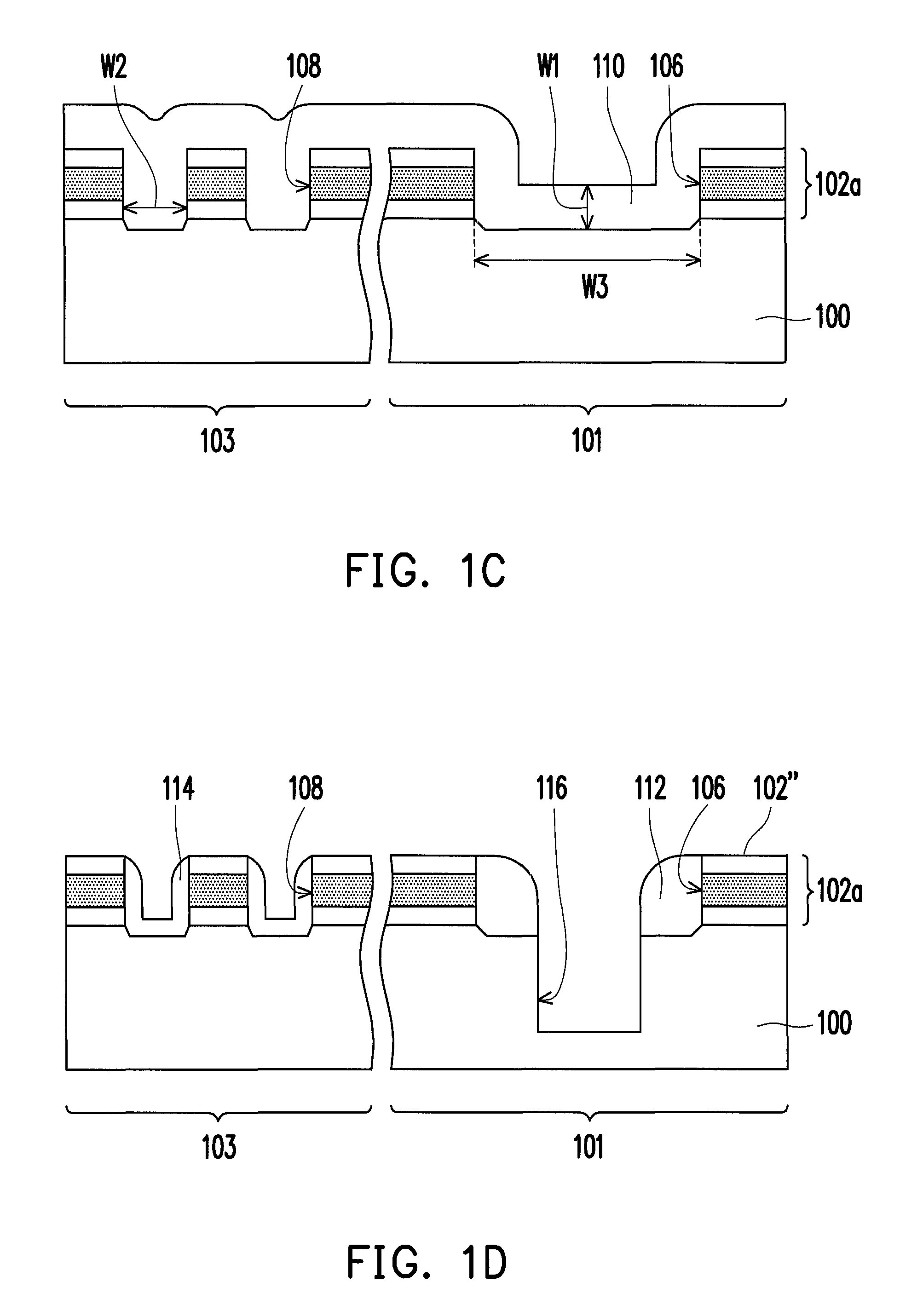
[0030]FIGS. 1A to 1H schematically illustrate cross-sectional views of a method of forming a semiconductor trench according to an embodiment of the present invention.

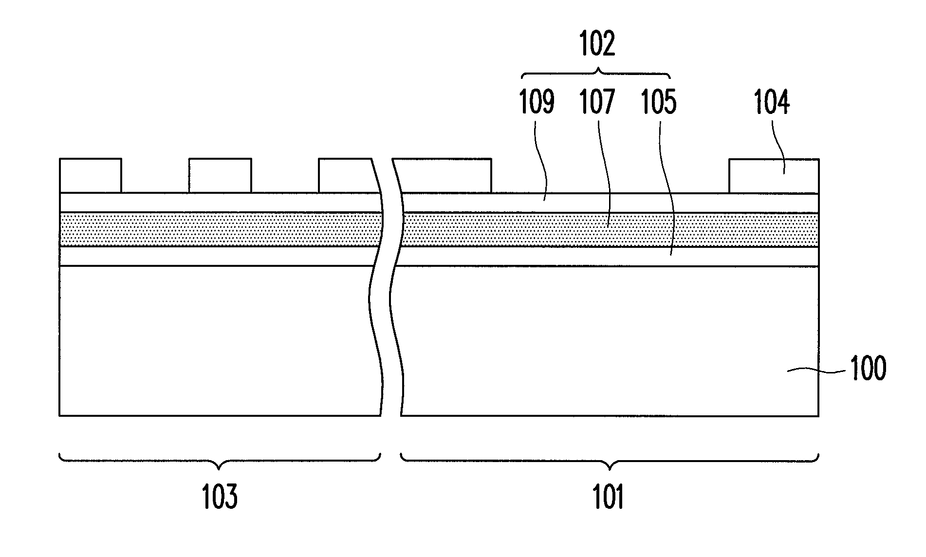
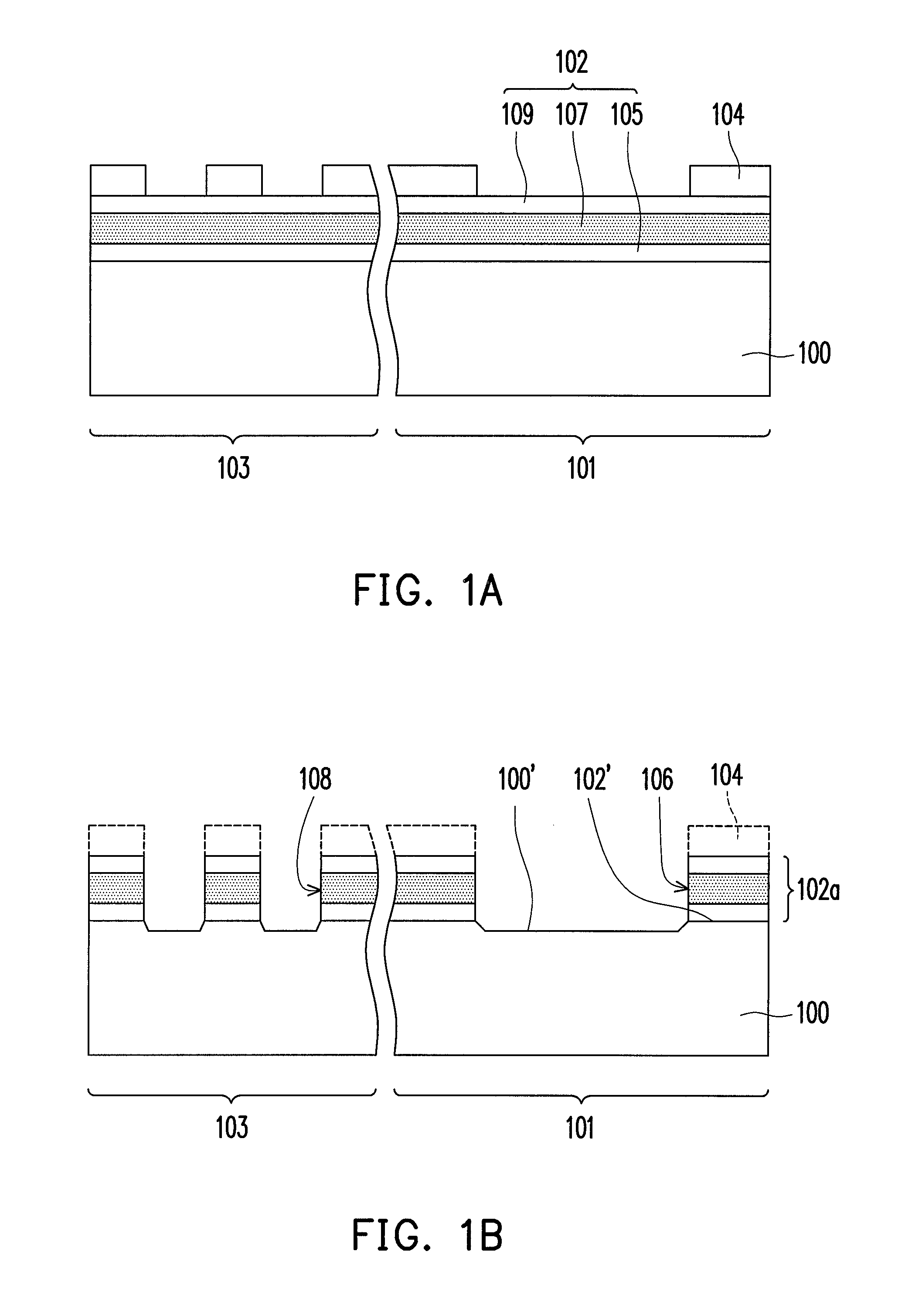
[0031]Referring to FIG. 1A, a substrate 100 is provided. The substrate 100 can be a semiconductor substrate such as a silicon substrate. The substrate 100 has a first area 101 and a second area 103. When the present invention is applied to a memory device, the first area 101 can be a periphery area and the second area 103 can be an array area. The periphery area 101 and the array area 103 are illustrated in the following for the purpose of clarity.

[0032]Thereafter, a mask material layer 102 and a patterned photoresist layer 104 are seque...


PUM


Abstract

Methods of forming a semiconductor trench and forming dual trenches and a structure for isolating devices are provided. The structure for isolating devices is disposed in a substrate having a periphery area and an array area. The structure for isolating devices includes a first isolation structure and a second isolation structure. The first isolation structure has a profile with at least three steps and is disposed in the substrate in the periphery area. The second isolation structure has a profile with at least two steps and is disposed in the substrate in the array area.

Description

BACKGROUND OF THE INVENTION[0001]1. Field of Invention[0002]The present invention relates to a semiconductor structure and a manufacturing method thereof, and more generally to dual isolation structures or dual trenches having different depths and a manufacturing method thereof.[0003]2. Description of Related Art[0004]Due to the rapid development of integrated circuit technologies, device miniaturization and integration become the major trends in the semiconductor manufacturing industry. As the dimension of a device continues to shrink and the level of integration continues to increase, a structure for isolating devices is required to reduce accordingly. Hence, with device miniaturization, isolation structures are increasingly difficult to fabricate.[0005]Because a shallow trench isolation (STI) structure is scalable without causing any bird's beak encroachment problem as in the conventional local oxidation of silicon (LOCOS) process, it is the preferred isolation technique for a su...

Claims


Application Information

Patent Timeline
Patent Type & Authority Patents(United States)
IPC IPC(8): H01L21/331
CPCH01L21/76229H01L21/76232
Inventor MA, CHU-MINGWU, TIN-WEIYANG, CHIH-HSIANG
Owner MACRONIX INT CO LTD
Why Eureka
Try Eureka