

Navigation and sample processing using an ion source containing both low-mass and high-mass species
a particle beam and ion source technology, applied in the direction of material analysis, instruments, nuclear engineering, etc., can solve the problems of not being able to use for actual ce, limiting image, and limiting ce applications
- Summary
- Abstract
- Description
- Claims
- Application Information
AI Technical Summary
Benefits of technology
Problems solved by technology
Method used
Image

Examples
Embodiment Construction
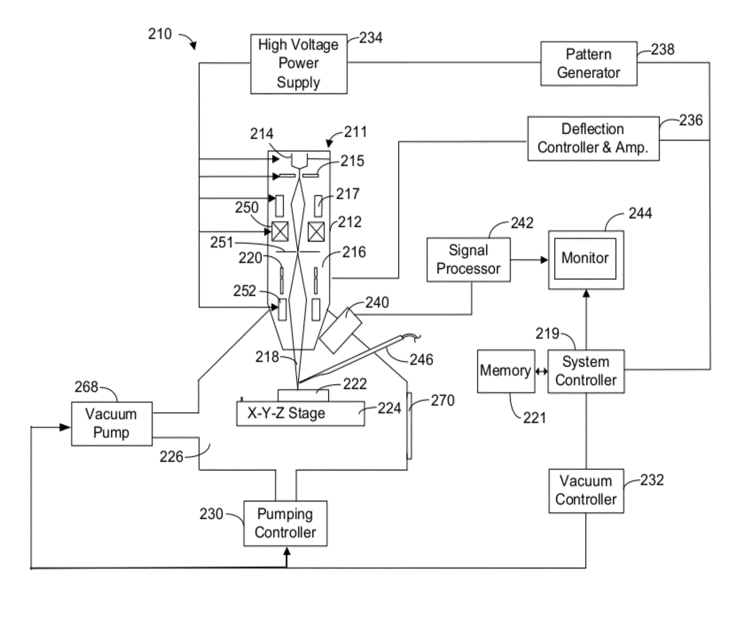
[0031]Preferred embodiments of the present invention are directed at methods of generating and using an ion beam composed of a mixture of light and heavy ions to provide imaging of subsurface features while still allowing for rapid material removal. In preferred embodiments of the present invention, the light and heavy ions are formed into a mixed beam so that they can be used simultaneously to process a sample, with the heavy ions milling the sample as in a conventional FIB system while the light ions penetrate deeper into the sample to provide information about subsurface features. In other preferred embodiments, a mass filter can be used to rapidly switch between light and heavy ions at a selected frequency to provide imaging of subsurface features while milling, and to also allow adjustment of the ratio of light and heavy ions produced by an alloy LMIS. A plasma FIB with multiple gas sources can also be used to practice the present invention, allowing the ratio of light and heav...
PUM
 Abstract
Description
Claims
Application Information