Circuit for amplifying a signal representing a variation in resistance of a variable resistance and corresponding sensor
a resistance and variable technology, applied in the field of circuits for amplifying signals representing resistance variations of variable resistors, can solve the problem that the most frequently used signal conditioning structures still consume a lot of current, and achieve the effect of reducing the structural complexity of the sensor and reducing the cost of the sensor
- Summary
- Abstract
- Description
- Claims
- Application Information
AI Technical Summary
Benefits of technology
Problems solved by technology
Method used
Image

Examples
first embodiment
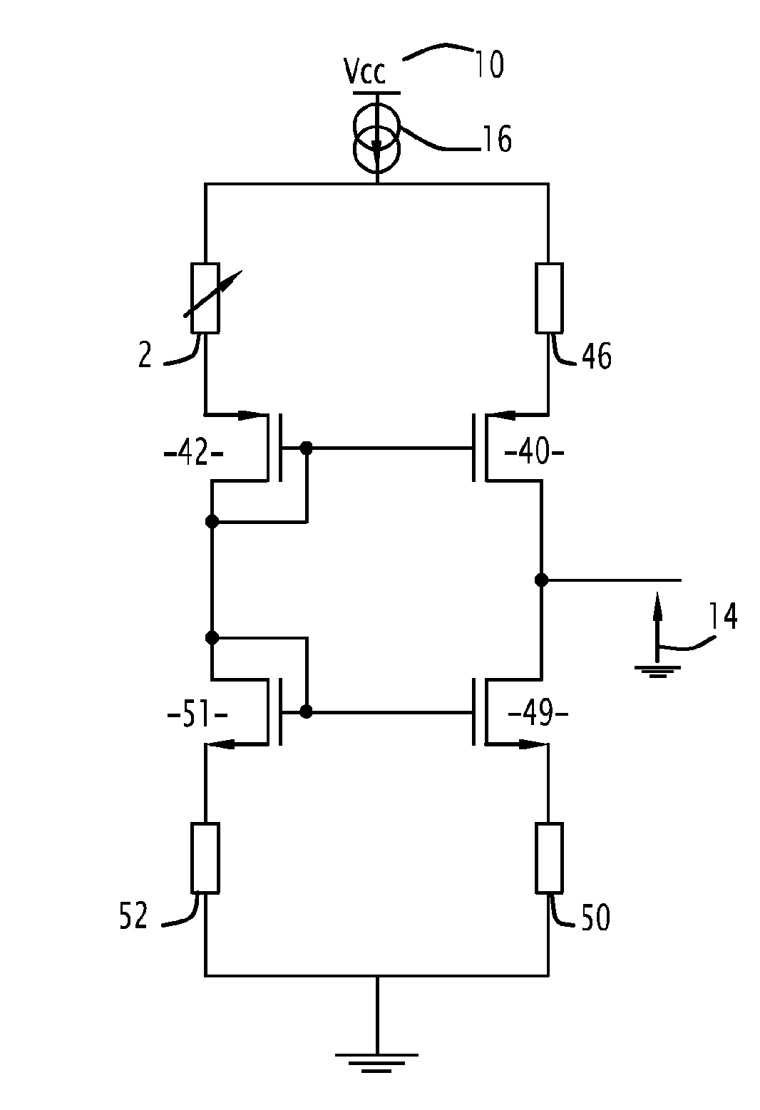
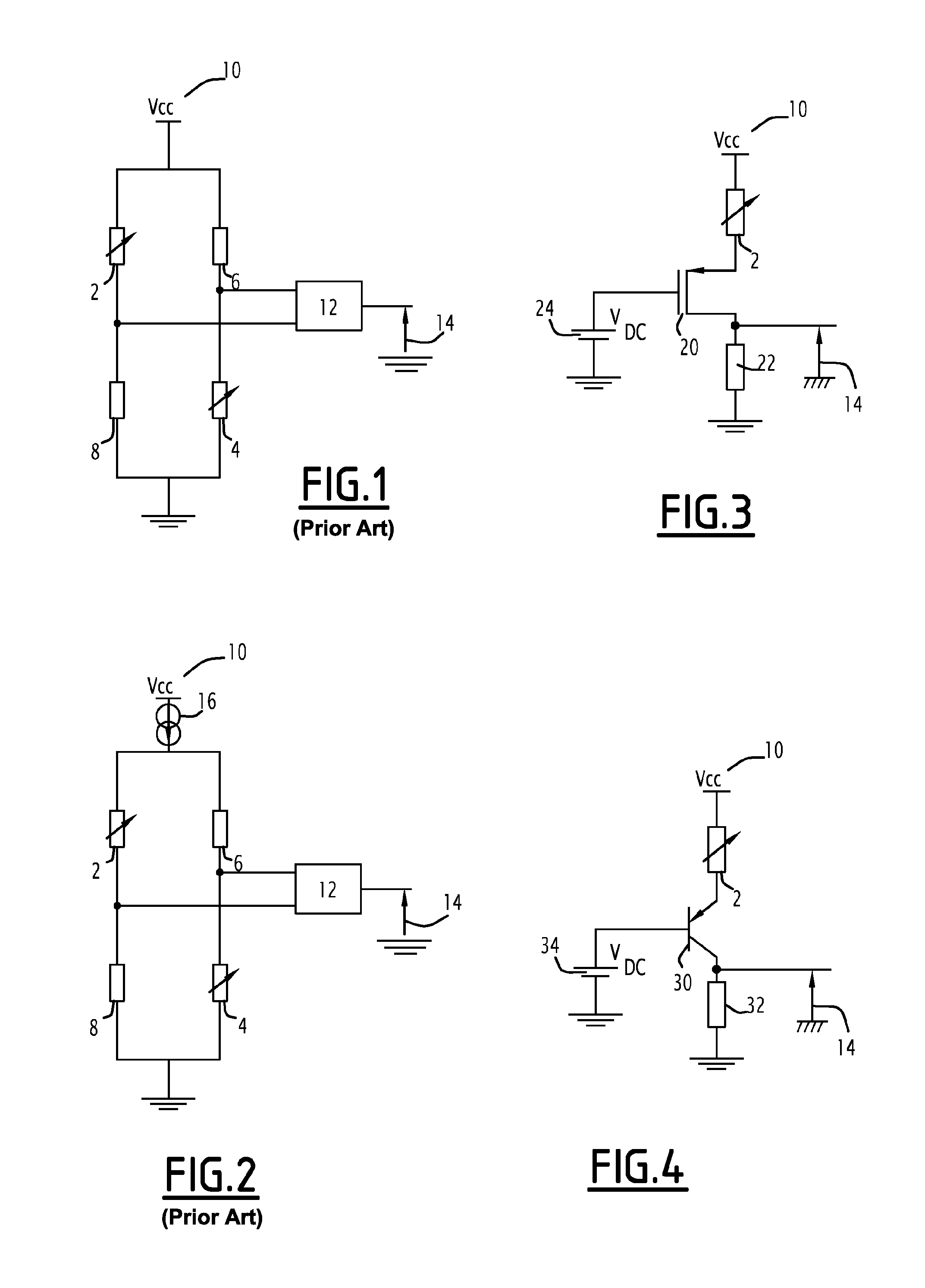
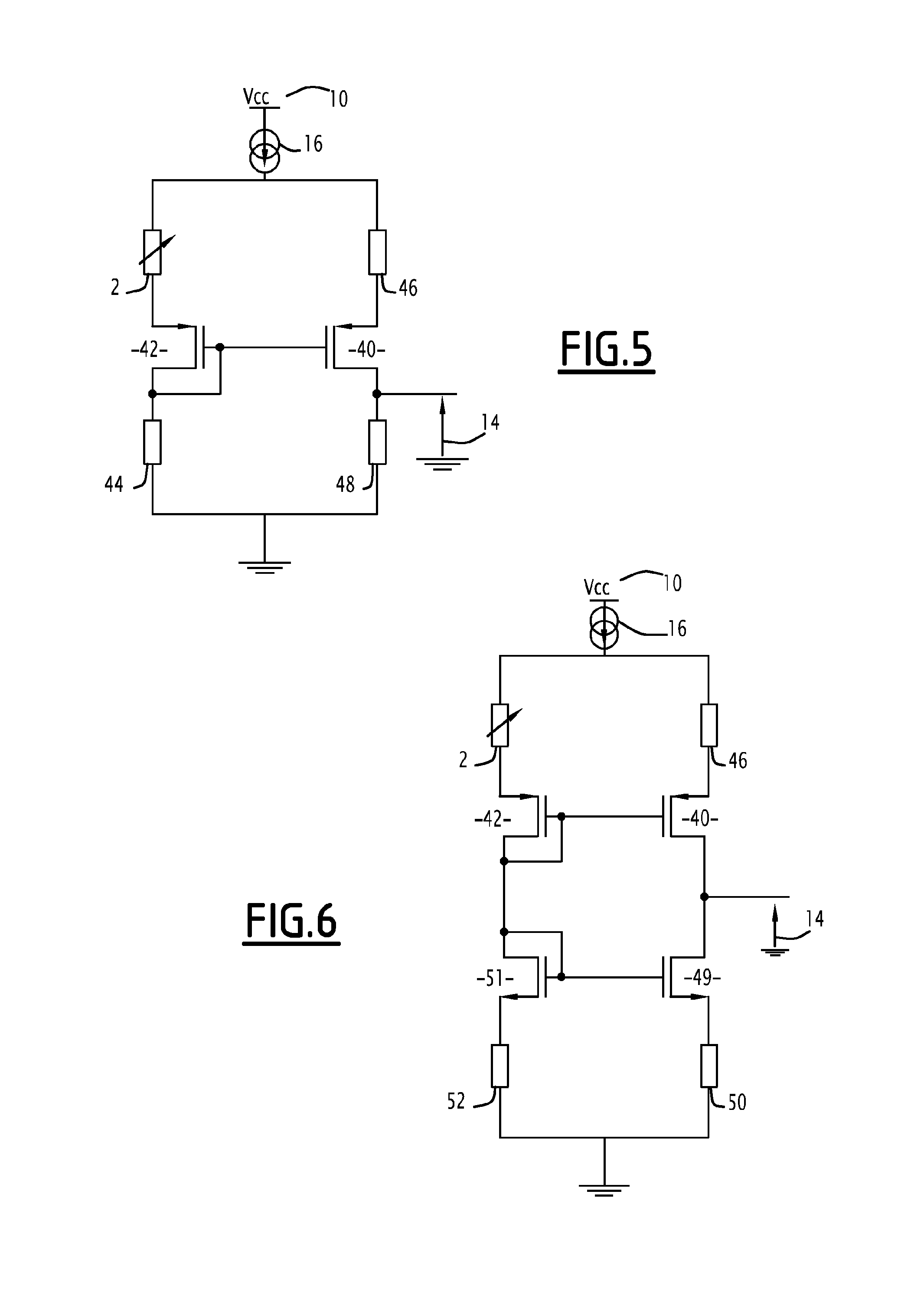
[0067]FIG. 3 shows such a circuit.
[0068]The circuit shown in FIG. 3 comprises a P-MOS field-effect transistor 20, the source of which is connected to the variable resistor 2 representing the sensitive element of the resistive sensor, the signal of which is to be recovered. The drain of the transistor 20 is connected to a load consisting of a reference resistor R1 denoted by the reference 22, at the terminals of which the amplified signal 14 is recovered. The gate of the transistor 20 is connected to a VDC direct voltage generator 24.
[0069]The variation ΔR in the variable resistor 2 causes a variation in voltage on the source of the transistor 20, thus allowing a modulation of the gate-source voltage VGS around an operating point.
[0070]The current consumed by the circuit of FIG. 3 is around a hundred microamperes for a resistance value of the variable resistor 2 equal to 1 kΩ. The current consumption of this circuit is therefore much lower than those of the conventional Wheatstone br...
second embodiment
[0071]FIG. 4 shows the circuit according to the invention.
[0072]The circuit shown in FIG. 4 comprises a PNP bipolar transistor 30, the emitter of which is connected to the variable resistor 2.
[0073]The collector of the transistor 30 is connected to a load consisting of a reference resistor R1 denoted by the reference 32, at the terminals of which the amplified signal 14 is recovered.
[0074]The base of the transistor 30 is connected to a VDC direct voltage generator 34.
[0075]The variation ΔR of the variable resistor 2 causes a variation in voltage on the emitter of the transistor 30, thus allowing a modulation of the base-emitter voltage VBE around an operating point.
[0076]The structures of FIGS. 3 and 4 are equivalents in terms of operation. Consequently, the embodiments described in the rest of the description concern circuits using MOS transistors, but they can be reproduced using bipolar transistors by making the analogy between the MOS transistor and the bipolar transistor in whi...
PUM
 Abstract
Description
Claims
Application Information
 - R&D
- Intellectual Property
- Life Sciences
- Materials
- Tech Scout
- Unparalleled Data Quality
- Higher Quality Content
- 60% Fewer Hallucinations
Browse by: Latest US Patents, China's latest patents, Technical Efficacy Thesaurus, Application Domain, Technology Topic, Popular Technical Reports.
© 2025 PatSnap. All rights reserved.Legal|Privacy policy|Modern Slavery Act Transparency Statement|Sitemap|About US| Contact US: help@patsnap.com