Supercharge Your Innovation With Domain-Expert AI Agents!

Method for monitoring the removal of polysilicon pseudo gates

a technology of pseudo gates and polysilicon, which is applied in the direction of individual semiconductor device testing, semiconductor/solid-state device testing/measurement, instruments, etc., can solve the problems of large negative impact of polycrystalline silicon residual on device performance, inability to directly monitor the removal process of pseudo gates, and complex process for 32 nm and even smaller technology nodes, so as to achieve fast, accurate, effective monitoring and determination, no damage to the wafer

Active Publication Date: 2013-08-06
INST OF MICROELECTRONICS CHINESE ACAD OF SCI
View PDF6 Cites 5 Cited by
  • Summary
  • Abstract
  • Description
  • Claims
  • Application Information

AI Technical Summary

Benefits of technology

[0006]In consideration of the aforementioned, the present invention discloses a method for monitoring the removal of a polycrystalline silicon dummy gate, to quickly, accurately, and effectively monitor and determine whether the polycrystalline silicon dummy gate has been thoroughly removed, and in the meantime, the method leads to no damage to the wafer.
[0015]This patent discloses two lines for monitoring the removal of the polycrystalline silicon dummy gate, and a method to examine if the dummy gate is thoroughly removed or not by detecting the wafer mass or mass difference. According to the measurement method of the present invention, the full wafer may be quickly and accurately measured without a specific test structure, to effectively monitor and determine whether the polycrystalline silicon dummy gate is thoroughly removed, meanwhile said measurement method gives a feedback quickly and accurately without causing any damage to the wafer.

Problems solved by technology

Because polycrystalline silicon residual will have a big negative impact on the device performance.
The process is a complex process for 32 nm and even smaller technology node.
But such a method is a destructive method, and feedback is often slow, so this method cannot be directly used to effectively monitor dummy gate removal process, especially in the mass production process.
With the technology nodes further scaling down, device structure and film stack composed of thinner films have become more complex.
The traditional optical detection methods are not able to quickly and accurately monitor the fine trench structure after dummy gate removal.

Method used


Image

  • Method for monitoring the removal of polysilicon pseudo gates
  • Method for monitoring the removal of polysilicon pseudo gates

Examples


embodiment 1

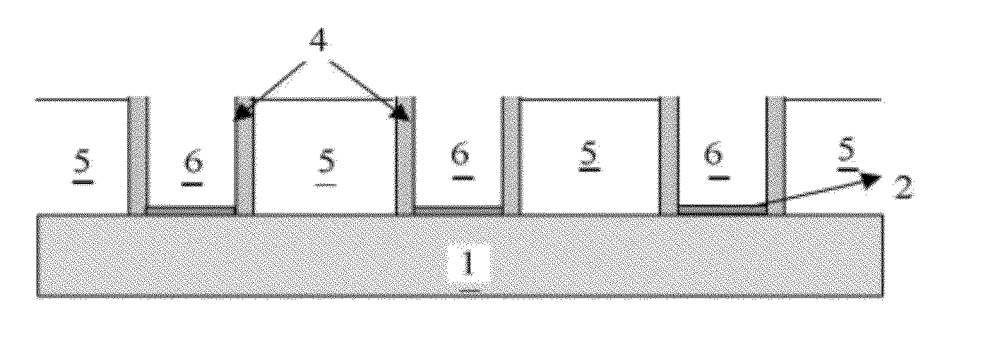
[0021]An insulating layer 2, polysilicon dummy gates 3, gate sidewalls 4, and an interlayer dielectric layer (ILD) 5 are sequentially formed on substrate 1, as shown in FIG. 1. Then, the polycrystalline silicon dummy gates 3 are removed to form gate openings trench 6. It can be seen from FIG. 1 that the mass of the films on the wafer (that is, the sum of mass of the films of ILD5 on the surface of the wafer, sidewalls 4 and gate openings trench 6 in ILD5) will be significantly reduced after removing the polycrystalline silicon dummy gates 3. Thus, by monitoring the wafer mass, it can be determined whether the polycrystalline silicon dummy gates have been thoroughly removed. This method is a direct measurement technique, which results no damage for the wafer and have a high measuring efficiency. Hence the method is appropriate to effectively monitor the process of the removal of the polycrystalline silicon dummy gates.

[0022]Specifically, the method for monitoring the removal of polyc...

embodiment 2

[0028]The method for monitoring the removal of polycrystalline silicon dummy gates in the gate last process in accordance with another embodiment of the present invention, comprises the steps of:

[0029]First, a polycrystalline silicon dummy gate structure is formed on a surface of a wafer. As shown in FIG. 1, a polycrystalline silicon dummy gate structure is formed on the surface of the wafer, that is, an insulating layer 2, polycrystalline silicon dummy gates 3, gate sidewalls 4, and interlayer dielectric layer (ILD) 5 are sequentially formed on a substrate 1. Then, the polycrystalline silicon dummy gates 3 are removed to form gate openings trench 6.

[0030]Second, a measurement target and an error range are determined. Polycrystalline silicon dummy gates may be formed on a wafer for testing purpose (i.e., a spare wafer which will not be finally cut into chips) according to the flow chart. Then a difference between the mass of a wafer of a certain product model (a destructive SEM or T...

embodiment 3

[0034]Similar to embodiment 1 or 2, the distinction only lies in whether the insulating layer 2 is a gate dielectric layer in the gate last process. If the insulating layer 2 includes a high-k material and is used as a gate dielectric layer in the gate last process, then in the monitoring method disclosed in the present invention, the insulating layer 2 will not be removed after the removal of polycrystalline silicon dummy gates 3, and it will be reserved. The monitoring method is the same. However, if the insulating layer 2 is merely used as an etch stop layer for the polycrystalline silicon gates 3, that is, the material for the insulating layer 2 being a common insulating dielectric material such as silicon dioxide, the insulating layer 2 shall be removed together with the polycrystalline silicon dummy gates 3, thus the above two embodiments of the present invention shall be modified accordingly.

[0035]Specifically, the varied monitoring methods of embodiment 3 with respect to emb...


PUM


Abstract

The present invention discloses a method for monitoring the removal of a polycrystalline silicon dummy gate, comprising the steps of: forming a polycrystalline silicon dummy gate structure on a surface of a wafer; determining a measurement target and an error range of mass of the wafer; and measuring the mass of the wafer by a mass measurement tool after polycrystalline silicon dummy gate removal to determine whether the polycrystalline silicon dummy gate has been completely removed. According to the measurement method of the present invention, the full wafer may be quickly and accurately measured without requiring a specific test structure, to effectively monitor and determine whether the polysilicon dummy gate is thoroughly removed, meanwhile said measurement method gives feedback directly, quickly and accurately without causing any damage to the wafer.

Description

CROSS REFERENCE[0001]This application is a National Stage Application of, and claims priority to, PCT Application No. PCT / CN2011 / 001992, filed on Nov. 29, 2011, entitled “METHOD FOR MONITOR THE REMOVAL OF POLYCRYSTALLINE SILICON DUMMY GATES”, which claims priority to Chinese Application No. 201110165279.5,0, filed on Jun. 20, 2011. Both the PCT application and the Chinese application are incorporated herein by reference in their entireties.FIELD OF THE INVENTION[0002]The present invention relates to a method for manufacturing a semiconductor device, particularly to a method for monitoring the removal of polycrystalline silicon dummy gates in the device manufacturing process.BACKGROUND OF THE INVENTION[0003]The successful implementation of high-k metal-gate (HKMG) in the 45 nm technology node has made it a necessary step in the key process flow for the sub-30 nm technology node. Intel, who has committed to a high-k metal-gate-last approach, is now the leader in mass production of 45 ...

Claims


Application Information

Patent Timeline
Patent Type & Authority Patents(United States)
IPC IPC(8): H01L21/66
CPCH01L22/12H01L29/66545
Inventor YANG, TAOZHAO, CHAOLI, JUNFENGYAN, JIANGCHEN, DAPENG
Owner INST OF MICROELECTRONICS CHINESE ACAD OF SCI
Features
  • R&D
  • Intellectual Property
  • Life Sciences
  • Materials
  • Tech Scout
  • Unparalleled Data Quality
  • Higher Quality Content
  • 60% Fewer Hallucinations
Learn More