Multi-layer substrate with a via hole and electronic device having the same

a multi-layer substrate and electronic device technology, applied in the direction of cross-talk/noise/interference reduction, printed circuit aspects, printed circuit manufacturing, etc., can solve the problems of signal distortion, noise generation, and reduce so as to improve the signal transmitting ability of the signal line

Inactive Publication Date: 2013-08-06
SAMSUNG ELECTRONICS CO LTD
View PDF25 Cites 12 Cited by
  • Summary
  • Abstract
  • Description
  • Claims
  • Application Information

AI Technical Summary

Benefits of technology

[0010]The present general inventive concept provides a multi-layer substrate and an electronic device having the same minimizing discontinuity of a return current path.
[0011]The present general inventive concept also provides a multi-layer substrate and an electronic device having the same which prevents an EMI radiation in a signal via hole, and improves a signal transmitting ability of a signal line.

Problems solved by technology

However, in the conventional multi-layer substrate, a signal distortion is generated due to discontinuity of the return current, and noise is generated at the multi-layer substrate which increases an electromagnetic in reference (EMI), etc.
Also, EMI is radiated in a radial direction of a via hole to have an effect on other signals, thereby reducing a signal transmitting ability.

Method used


Image

  • Multi-layer substrate with a via hole and electronic device having the same
  • Multi-layer substrate with a via hole and electronic device having the same
  • Multi-layer substrate with a via hole and electronic device having the same

Examples


Embodiment Construction

[0050]Reference will now be made in detail to the embodiments of the present general inventive concept, examples of which are illustrated in the accompanying drawings, wherein reference numerals refer to their respective elements throughout. The embodiments are described below so as to explain the present general inventive concept by referring to the figures.

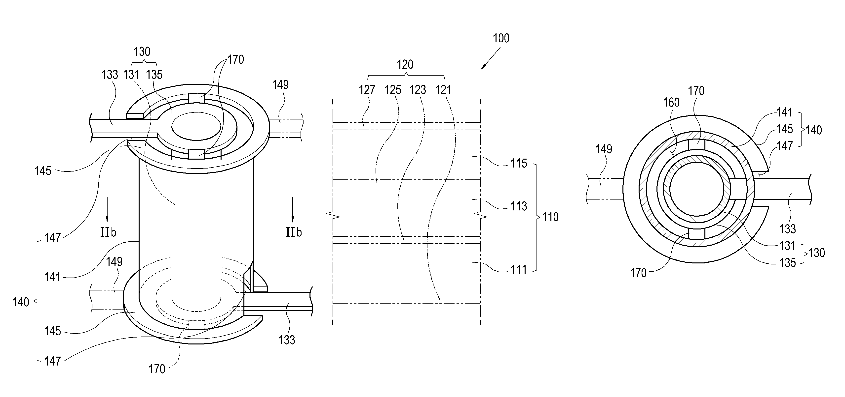
[0051]As illustrated in FIGS. 2A to 7B, a multi-layer substrate 100 according to a few examples of an exemplary embodiment of the present general inventive concept includes a signal via hole 130 and a sub via hole 140. The multi-layer substrate 100 includes a plurality of substrate main bodies 110 and layers 120 layered in sequence. The multi-layer substrate 100 may include a surface mounted device (SMD) mounted on a surface of the layers 120 to perform various functions. The multi-layer substrate 100 may include a plurality of layers, such as six layers, eight layers, etc, as well as four layers according to examples of the pre...


PUM


Abstract

A multi-layer substrate includes a plurality of substrate main bodies, a plurality of layers which are alternately layered with the main bodies, a signal via hole which is connected with a signal line and includes a signal column which passes through at least one substrate main body; and a sub via hole which includes a sub column which surrounds the signal column, and a pair of sub pads which extend from end parts of the sub column to be formed to the layers, the layers which are formed with the sub pads being disposed in the same layer as the layers which are formed with the signal line of the signal via hole, or being disposed outside the layers which are formed with the signal line which is connected with the signal via hole.

Description

CROSS-REFERENCE TO RELATED APPLICATIONS[0001]This application claims priority from Korean Patent Application No. 10-2007-0003295, filed on Jan. 11, 2007 in the Korean Intellectual Property Office, the disclosure of which is incorporated herein by reference in its entirety.BACKGROUND OF THE INVENTION[0002]1. Field of the Invention[0003]A multi-layer substrate and an electronic device having the same consistent with the present general inventive concept relate to improving a return current path of a signal line.[0004]2. Description of the Related Art[0005]In general, a substrate is widely used as a component of an electronic device from a home appliance such as a digital TV, a computer, etc. to a high technology communicating device. The substrate forms a signal line on a predetermined main body to couple electrical components such as an integrated circuit, a resistor, a switch, etc., or signal lines, thereby electrically connecting or transmitting a signal.[0006]The substrate is clas...

Claims


Application Information

Patent Timeline
Patent Type & Authority Patents(United States)
IPC IPC(8): H05K1/11
CPCH05K1/0219H05K2201/09809H05K3/429H05K3/46
Inventor KIM, YOUNG-SEOK
Owner SAMSUNG ELECTRONICS CO LTD
Why Eureka
Try Eureka