

Solid-state image sensor
a solid-state image and sensor technology, applied in the field of solid-state image sensors, can solve the problems of difficult to realize such a structure, provide a structure, and spread of light, and achieve the effects of reducing crosstalk, excellent color reproducibility, and high definition capabilities
- Summary
- Abstract
- Description
- Claims
- Application Information
AI Technical Summary
Benefits of technology
Problems solved by technology
Method used
Image

Examples
embodiment 1
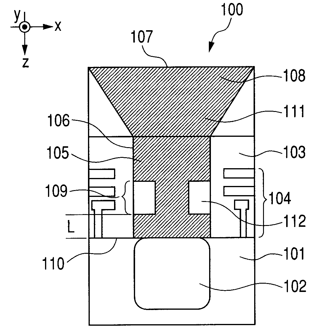
[0026]The solid-state image sensor of Embodiment 1 of the present invention will be described by referring to FIG. 1A. The solid-state image sensor of this embodiment includes pixel units having a substrate including a photoelectric conversion section in the inside and an optical waveguide arranged at the light incident side of the substrate so as to lead incident light converted into the guided mode that the optical waveguide possesses and being propagated through the optical waveguide to the photoelectric conversion section.
[0027]More specifically, the solid-state image sensor of this embodiment includes a plurality of pixel units 100 arranged to form a matrix. Each of the pixel units 100 has a silicon substrate 101 and a photoelectric conversion section 102 arranged in the inside of the silicon substrate 101. Additionally, the pixel unit 100 has a clad section (interlayer insulating section) 103 formed of a transparent material on the silicon substrate 101 and a wiring section 10...
embodiment 2
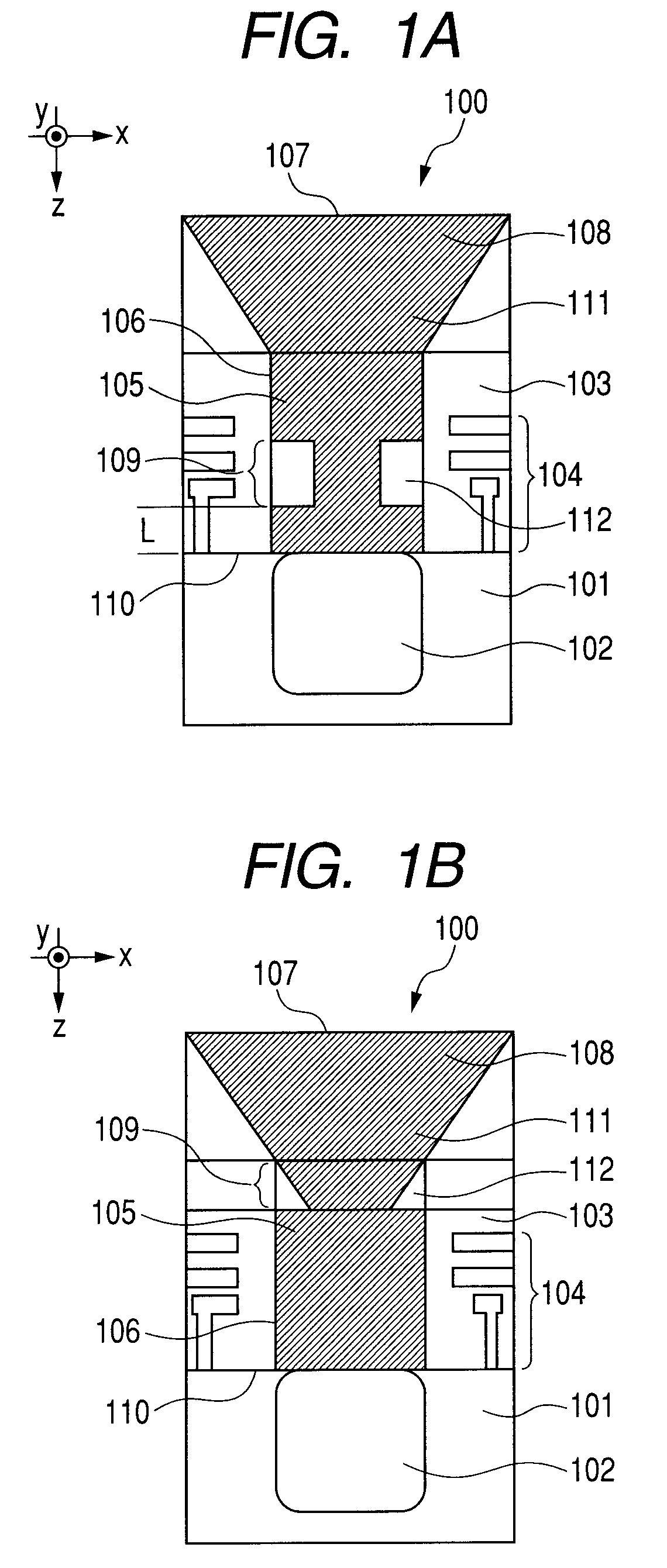
[0080]Now, the solid-state image sensor of Embodiment 2 of the present invention will be described below by referring to FIG. 9A. The solid-state image sensor of this embodiment includes a plurality of pixel units 200 arranged in the form of a matrix. The pixel units 200 of this embodiment have a structure that differs from the pixel unit 100 of Embodiment 1 illustrated in FIG. 1A only in terms of the mode conversion section. If the refractive index of the core section 105 is n1 and the refractive index of the clad section 103 is n2, the mode conversion section 201 is formed by arranging a mode conversion structure 202 having refractive index n3 (105 in the optical waveguide 106. Note that it is sufficient for the mode conversion structure 202 to be made of a material having a refractive index different from the core section 105. It is assumed here that the mode conversion structure 202 has a refractive index lower than that of the core section 105. Assume that the width of the core...
embodiment 3
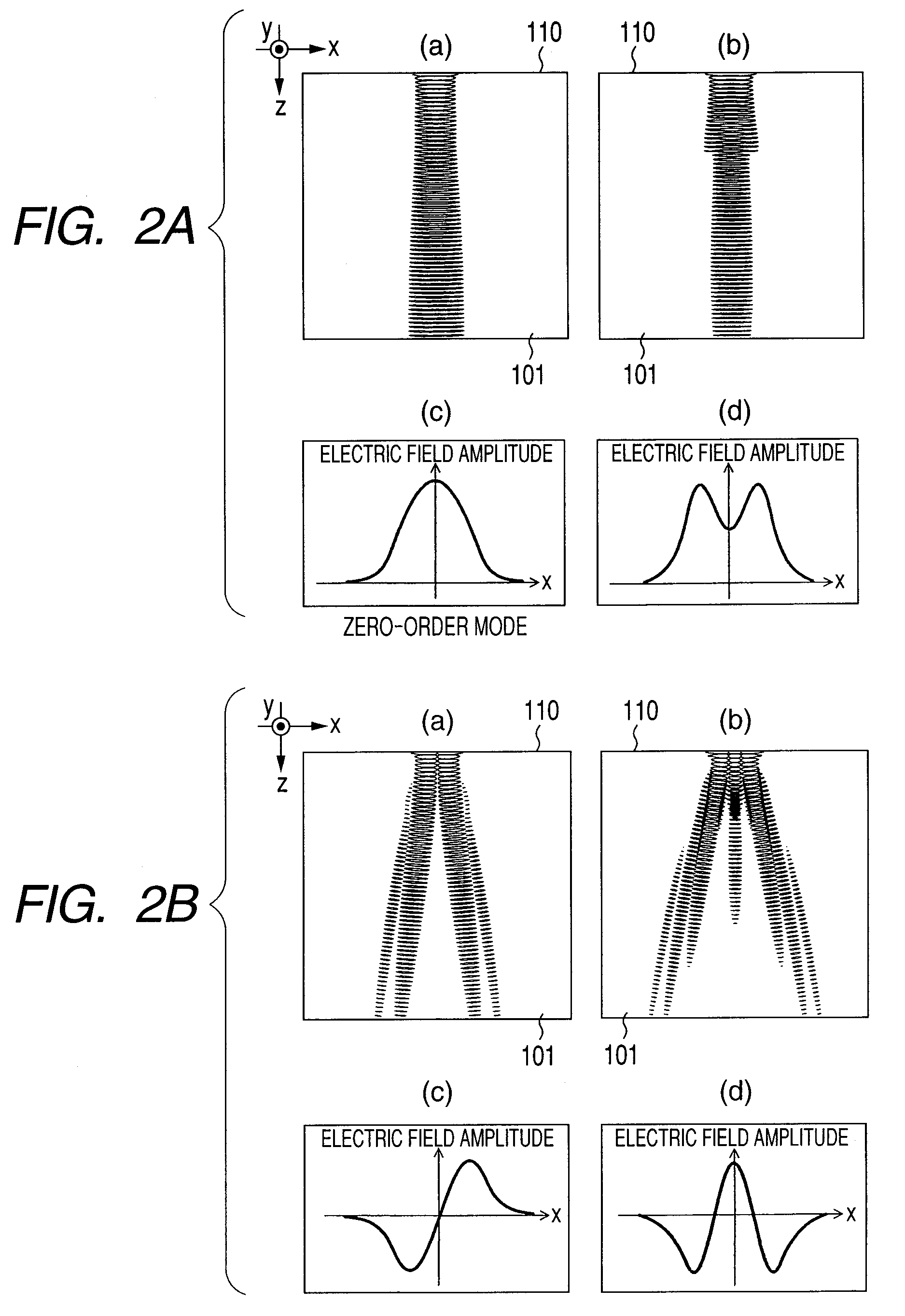
[0095]The solid-state image sensor of Embodiment 3 of the present invention will be described below by referring to FIG. 13A. The solid-state image sensor of this embodiment includes a plurality of pixel units 300 arranged in the form of a matrix. Unlike the pixel unit 100 of Embodiment 1 illustrated in FIG. 1A, the mode conversion structure 112 of the mode conversion section 109 of the pixel units 300 of this embodiment is made of metal. In FIGS. 1A and 13A, the components having a same function are denoted by a same reference symbols. In this embodiment, the optical waveguide 106 illustrated in FIG. 13A has eigenmodes same as those illustrated in FIG. 3A for Embodiment 1. Light entering the device from the incident surface 107 is converted into the guided mode that is expressed by superposing the eigenmodes for propagation. Light is propagated through the core section 105 in a concentrated manner so as to be protected against the crosstalk that arises on the silicon substrate 101....
PUM
 Abstract
Description
Claims
Application Information