

Logic built-in self-test programmable pattern bit mask
a logic and self-testing technology, applied in the direction of electronic circuit testing, measurement devices, instruments, etc., can solve the problems of less effective lbist testing in production, failure of integrated circuit logic to correspond,
- Summary
- Abstract
- Description
- Claims
- Application Information
AI Technical Summary
Benefits of technology
Problems solved by technology
Method used
Image

Examples
first embodiment
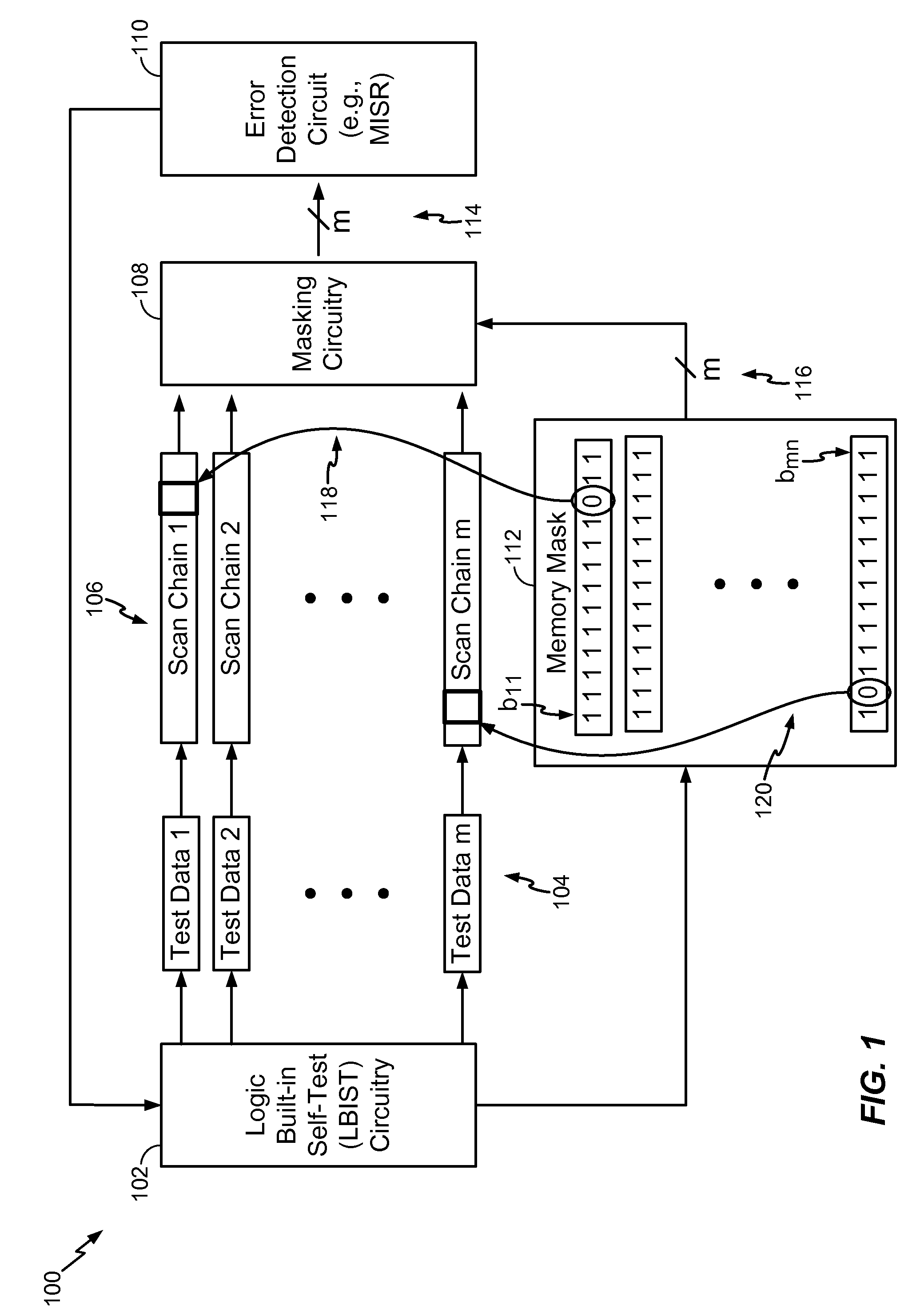
[0016]Particular embodiments of the present disclosure are described with reference to the drawings. In the description, common features are designated by common reference numbers. Referring to FIG. 1, an illustrative block diagram of a logic built-in self-test (LBIST) testing system having a memory mask applied to sub-portions of multiple scan chains is depicted and generally designated 100. The LBIST testing system 100 includes LBIST circuitry 102 coupled to m sets of test data 104. The m sets of test data 104 are coupled to m scan chains 106. The m scan chains 106 are coupled to masking circuitry 108. The masking circuitry 108 is coupled to an error detection circuit 110, such as a multiple input shift register (MISR), which is coupled to the LBIST circuitry 102. The LBIST circuitry 102 is also coupled to a memory mask 112. The memory mask 112 is coupled to the masking circuitry 108 via an m-bit line 116. The masking circuitry 108 is coupled to the error detection circuit 110 via...
second embodiment
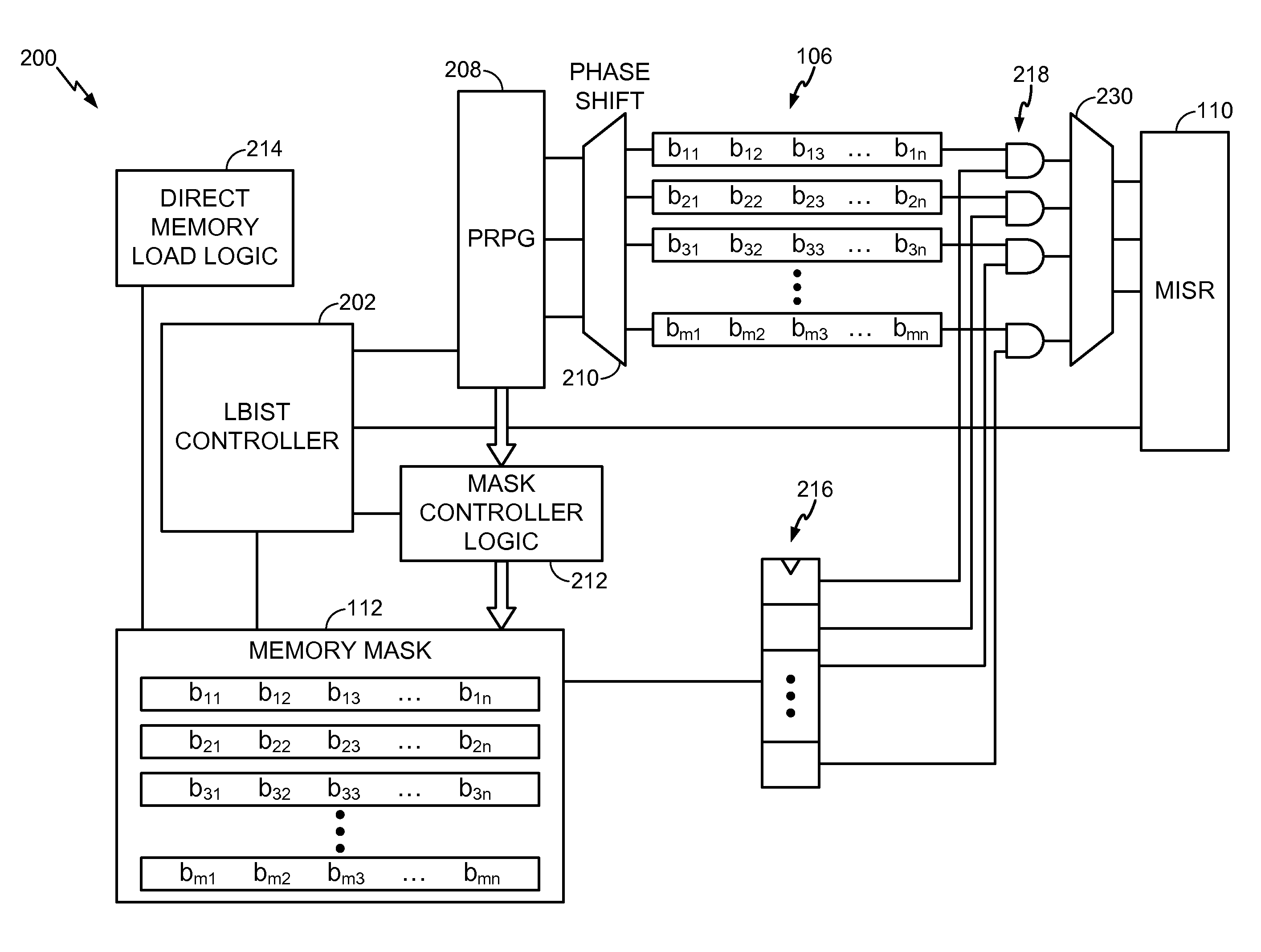
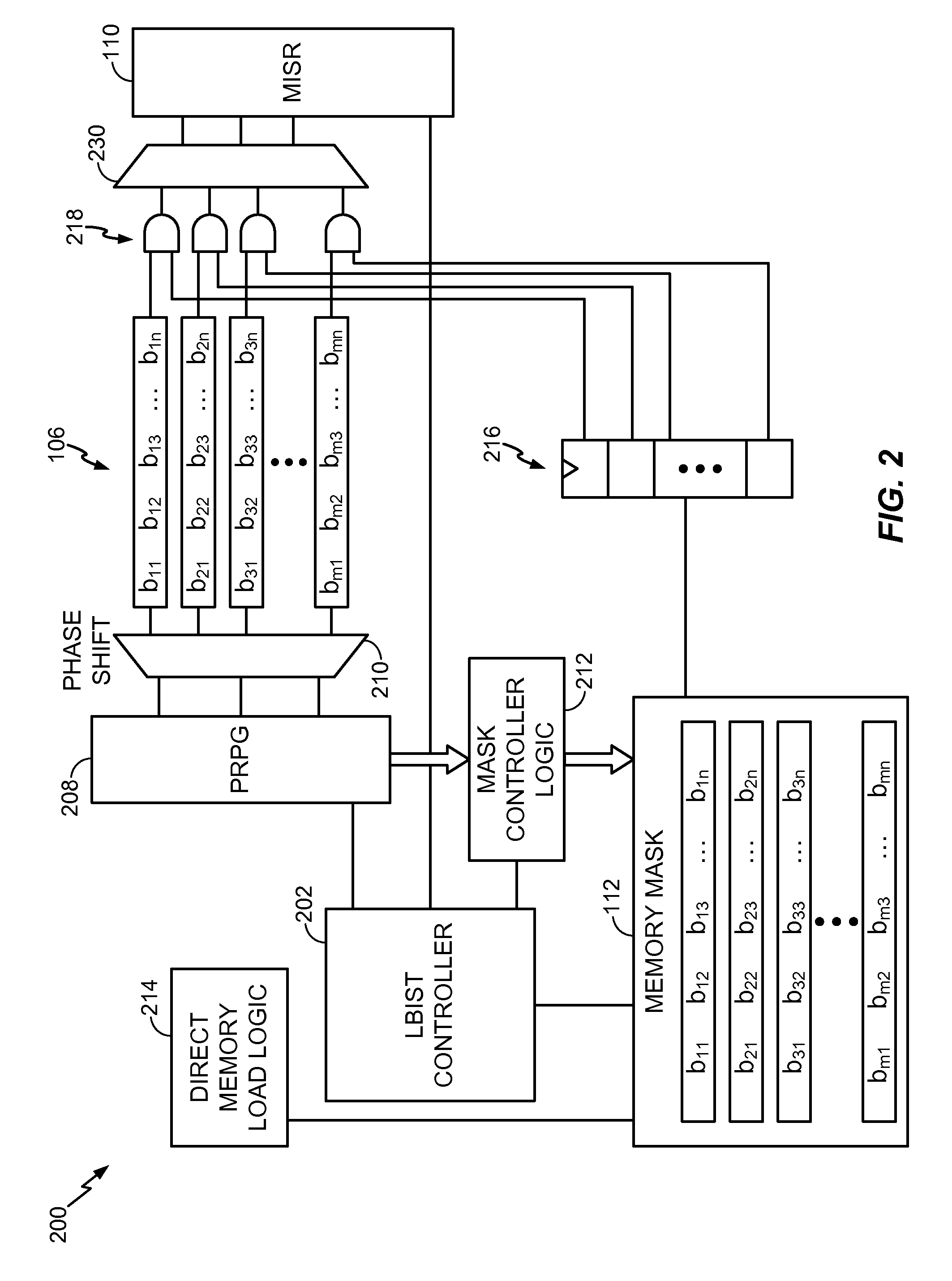
[0022]Referring to FIG. 2, an illustrative block diagram of a logic built-in self-test (LBIST) testing system having a memory mask applied to sub-portions of multiple scan chains is depicted and generally designated 200. The LBIST testing system 200 includes an LBIST controller 202 coupled to a memory mask 112. The LBIST controller 202 is also coupled to mask controller logic 212, which is also coupled to the memory mask 112. The LBIST controller 202 is further coupled to a pseudo-random pattern generator (PRPG) 208, which is coupled to a phase shift device 210. The PRPG 208 is coupled to the mask controller logic 212. The LBIST controller 202 is also coupled to a multiple input shift register (MISR) 110.
[0023]The phase shift device 210 is coupled to a set of m scan chains 106. The phase shift device 210 may be configured to modify data generated by the PRPG 208 to reduce correlations between different sets of scan chain data. For example, the phase shift device 210 may include an e...
third embodiment
[0029]Referring to FIG. 3, an illustrative block diagram of a logic built-in self-test (LBIST) testing system having a memory mask applied to sub-portions of multiple scan chains is depicted and generally designated 300. The LBIST testing system 300 includes the LBIST testing system 200 of FIG. 2 and joint test action group (JTAG) logic 322. Joint test action group (JTAG) logic 322 is coupled to the memory mask 112.
[0030]In a particular embodiment, the JTAG logic 322 may be used to map the failing bit positions within the m scan chains 106 to the memory locations in the memory mask 112. The JTAG logic 322 may access the memory locations in the memory mask 112 that correspond to the failing bit positions within the m scan chains 106 and set the values at the respective memory locations accordingly.
[0031]Referring to FIG. 4, a flow diagram of a first illustrative embodiment of a method of logic built-in self-test (LBIST) testing applying a memory mask to sub-portions of multiple scan ...
PUM
 Abstract
Description
Claims
Application Information