Fabrication and mask design methods using spatial frequency sextupling technique

Active Publication Date: 2013-09-03
VIGMA NANOELECTRONICS
View PDF4 Cites 39 Cited by
  • Summary
  • Abstract
  • Description
  • Claims
  • Application Information

AI Technical Summary

Benefits of technology

[0007]In the other process, minor modification is made to replace the amorphous carbon (first mandrel material in the former process) with a patterned resist and to use the second mandrel (spacer A) as a hard mask to transfer the spacer pattern to the layer underneath to avoid the problem of asymmetric spacer pr

Problems solved by technology

Unfortunately, the SADP mask design methodology does not work for a SASP process as it will result in a small gap between the second mandrels and spacer C. Such a small gap

Method used


Image

  • Fabrication and mask design methods using spatial frequency sextupling technique
  • Fabrication and mask design methods using spatial frequency sextupling technique
  • Fabrication and mask design methods using spatial frequency sextupling technique

Examples


Embodiment Construction

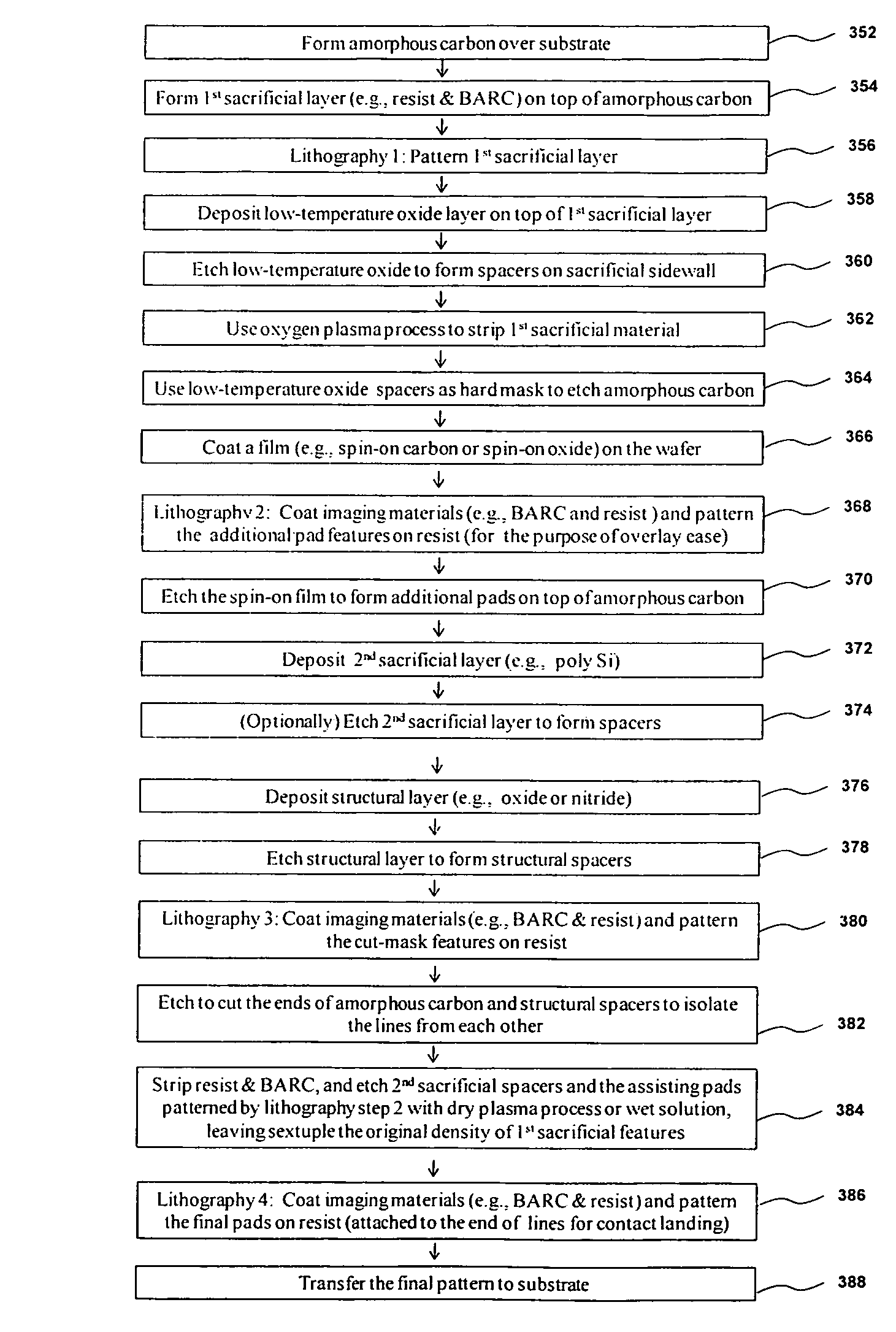
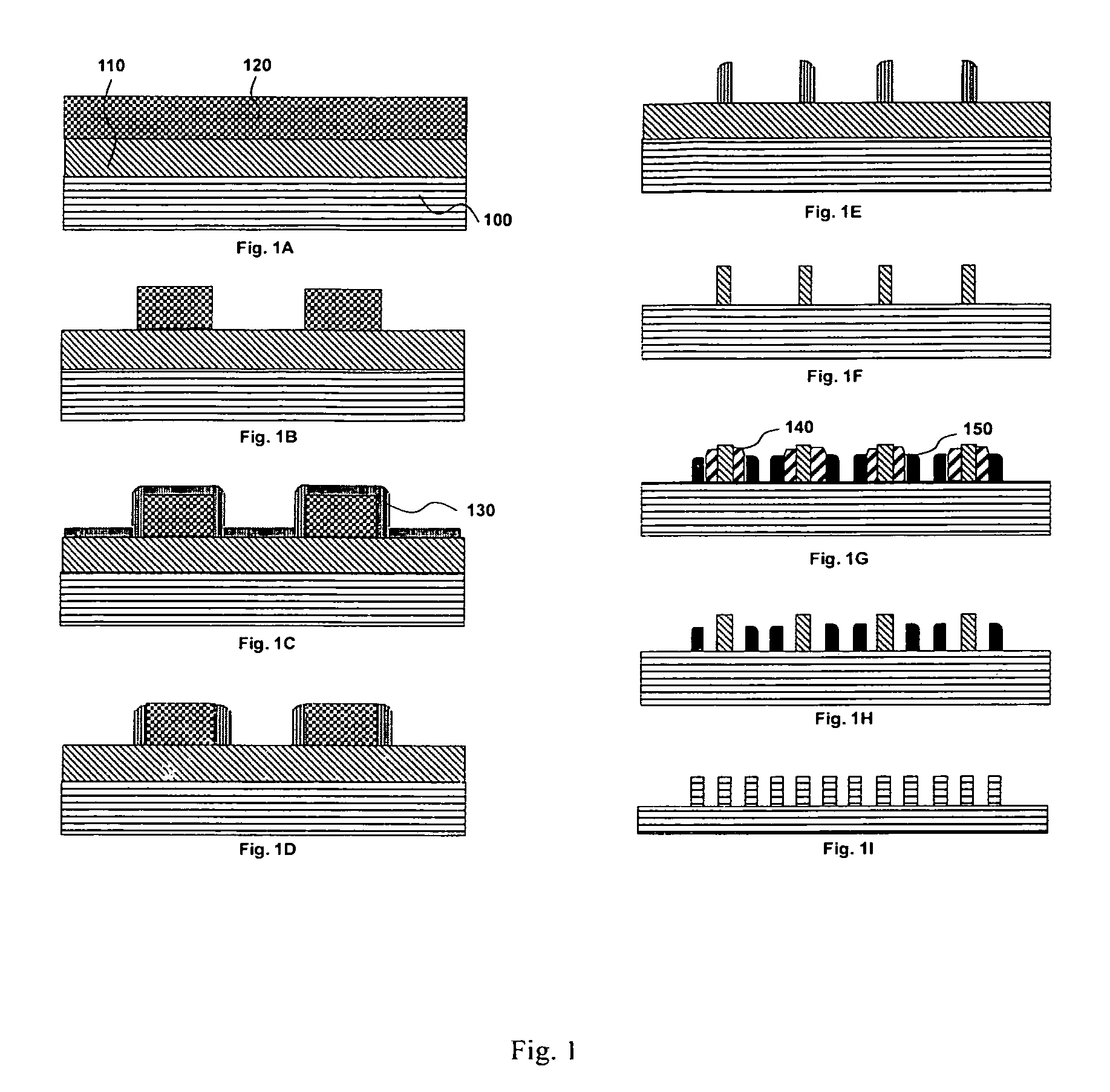
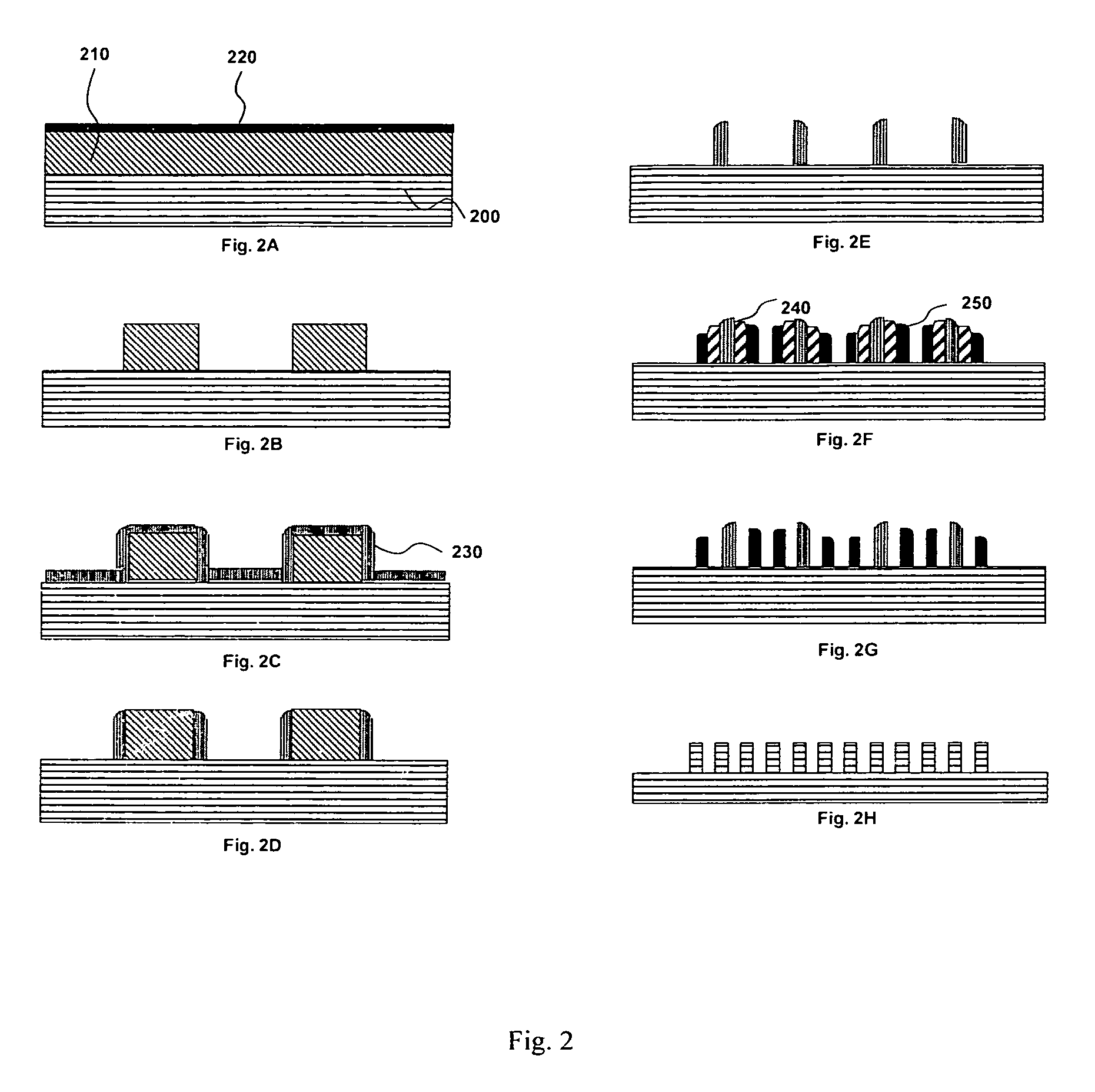
[0015]Embodiments of the present invention (self-aligned sextuple patterning, SASP) pertain to methods of forming patterned features on a substrate having a pitch reduced to one sixth of what is achievable using standard lithographic techniques. Compared with self-aligned double patterning (SADP) process which has been used in the production of high density 1-D lines / spaces, the SASP technique significantly increases the feature density by using a slightly more complex process. While this technique can form bit lines, wider lines and features (e.g., line-end pads, power supply lines, string select lines in NAND devices, etc.) are usually necessary on same layer to form working devices, which requires multiple masks to be used to pattern one critical layer. Therefore, it is important to research a mask design method that not only allows reasonable (i.e., not too tight) overlay specifications, but also requires the minimum number of masks to reduce the process complexity and costs.

[00...


PUM


Abstract

Self-aligned sextuple patterning (SASP) processes and mask design methods for the semiconductor manufacturing are invented. The inventions pertain to methods of forming one and/or two dimensional features on a substrate having the feature density increased to six times of what is possible using the standard optical lithographic technique; and methods to release the overlay requirement when patterning the critical layers of semiconductor devices. Our inventions provide production-worthy methods for the semiconductor industry to continue device scaling beyond 15 nm (half pitch).

Description

BACKGROUND OF THE INVENTION[0001]Optical ArF (wavelength: 193 nm) DUV immersion lithography with NA=1.35 can print half-pitch features as small as 38 nm. The next-generation EUV lithography (EUVL) technology has been delayed for several times due to its limitations in power source, throughput, resist line edge roughness (LER) and mask defect issues [1]. Therefore, a paradigm shift in patterning technology, from mainly relying on scanners' optical resolution capability to adopting spacer based frequency multiplication techniques, has occurred in the semiconductor industry to continue IC scaling.[0002]Spacer based self-aligned multiple patterning techniques [2-4] such as double (SADP), triple (SATP), quadruple (SAQP) schemes, when combined with ArF DUV immersion lithgraphy, can potentially drive the resolution of IC features down to about 10 nm (half pitch). By designing various mandrel patterns which further define the route of the spacers formed on their sidewall, some multiple patt...

Claims


Application Information

Patent Timeline
IPC IPC(8): H01L21/331
CPCH01L29/00H01L21/0337H01L21/0338
Inventor CHEN, YIJIAN
Owner VIGMA NANOELECTRONICS
Why Eureka
Try Eureka