Nonvolatile memory and methods for manufacturing the same with molecule-engineered tunneling barriers

a technology of nonvolatile memory and tunneling barriers, which is applied in the direction of digital storage, semiconductor devices, instruments, etc., can solve the problems of scaling roadblocks and limit the scalability of p/e voltage, and achieve the effect of increasing the retention time/program-erase time ratio

Active Publication Date: 2013-09-24
NANO C INC +1
View PDF12 Cites 1 Cited by
  • Summary
  • Abstract
  • Description
  • Claims
  • Application Information

AI Technical Summary

Benefits of technology

[0012]According to an aspect of the application, semiconductor devices can exhibit increased retention time / program-erase time ratios.

Problems solved by technology

However, this related art approach limits the scalability of the P / E voltage, which is quickly becoming the major scaling roadblock, considering power dissipation, cycling endurance, and peripheral circuitry design.

Method used


Image

  • Nonvolatile memory and methods for manufacturing the same with molecule-engineered tunneling barriers
  • Nonvolatile memory and methods for manufacturing the same with molecule-engineered tunneling barriers
  • Nonvolatile memory and methods for manufacturing the same with molecule-engineered tunneling barriers

Examples


Embodiment Construction

[0026]An exemplary process for fabricating exemplary embodiments of tunneling barriers, semiconductor structures, and semiconductor devices using the same will now be described. However, embodiments of the application is not intended to be so limited as additional processes may be utilized based on the resulting tunnel barriers achieving the functionality described herein.

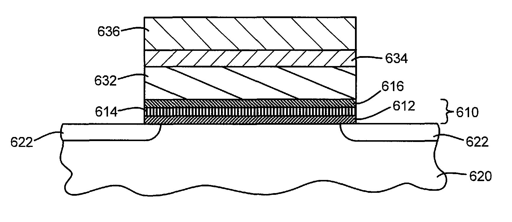
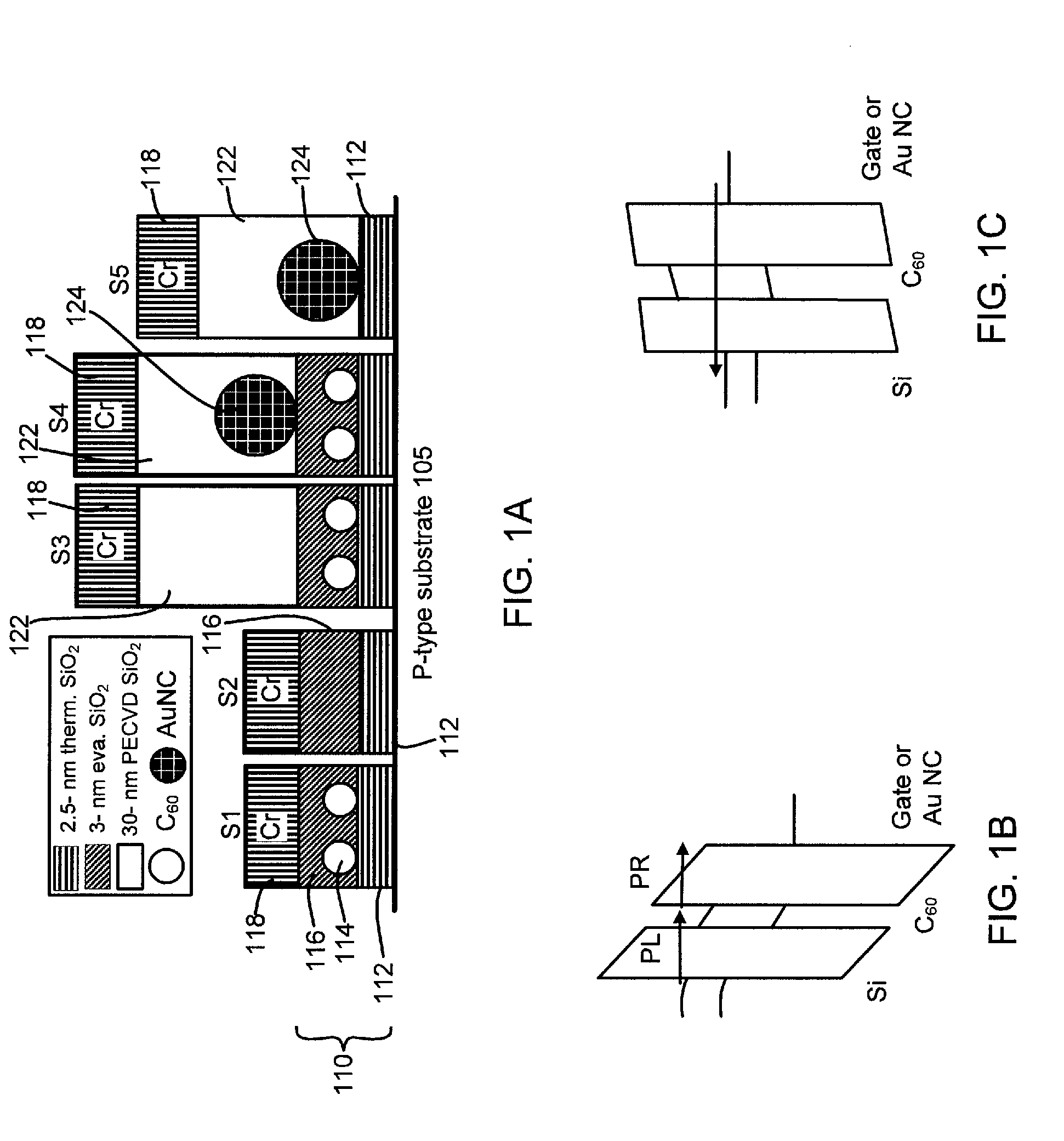
[0027]FIG. 1 is a diagram showing schematics of various exemplary heterogeneous semiconductor structure stacks (S1-S5), selective ones of which include exemplary embodiments of tunneling barriers according to the application. As shown in FIG. 1a, metal oxide semiconductor (MOS) capacitors with conventional local oxidation of Si (LOCOS) isolation on p-type semiconductor substrates were fabricated in one embodiment. After 2.5 nm dry thermal oxidation, C60 molecules were thermally evaporated to a thickness of 0.4 to 0.6 nm as measured by the quartz crystal monitor, followed by SiO2 evaporation of 3 nm to complete the ...


PUM


Abstract

Embodiments of tunneling barriers and methods for same can embed modules exhibiting a monodispersion characteristic into a dielectric layer (e.g., between first and second layers forming a dielectric layer). In one embodiment, by embedding C60 molecules inbetween first and second insulating layers forming a dielectric layer, a field sensitive tunneling barrier can be implemented. In one embodiment, the tunneling barrier can be between a floating gate and a channel in a semiconductor structure. In one embodiment, a tunneling film can be used in nonvolatile memory applications where C60 provides accessible energy levels to prompt resonant tunneling through the dielectric layer upon voltage application.

Description

CROSS REFERENCE TO RELATED APPLICATIONS[0001]This application claims the priority of U.S. Provisional Application No. 61 / 163,883, filed Mar. 27, 2009 entitled “Resonant Tunneling Barrier Using C60 For Tunnel Oxide In Flash Memory,” which is incorporated herein by reference in its entirety.STATEMENT REGARDING FEDERALLY SPONSORED RESEARCH OR DEVELOPMENT[0002]This invention was made with Government support under Grant Number EEC-0646547 awarded by the National Science Foundation. The United States Government has certain rights in the invention.FIELD OF THE INVENTION[0003]The present invention relates to tunneling barriers and / or semiconductor structures including tunneling barriers and methods for manufacturing the same.DESCRIPTION OF THE RELATED ART[0004]In the related art, charge-based nonvolatile flash memory technology, the ratio between retention time tR and program / erase (P / E) time tPE is about 1012-1014. To realize this tremendous ratio, field asymmetric tunneling processes in t...

Claims


Application Information

Patent Timeline
Patent Type & Authority Patents(United States)
IPC IPC(8): G11C11/34
CPCB82Y10/00H01L21/28273H01L21/28282H01L27/11521H01L27/11568G11C16/0466H01L29/40114H01L29/40117H10B43/30H10B41/30
Inventor KAN, EDWIN C.HOU, TUO-HUNG
Owner NANO C INC
Why Eureka
Try Eureka