Power semiconductor device

a technology of semiconductor devices and semiconductors, applied in semiconductor devices, semiconductor/solid-state device details, diodes, etc., can solve the problems of uneven thickness of film, difficult to ensure the focus margin in photolithography, and large film thickness, so as to reduce the unevenness of thickness and reduce the unevenness of characteristics

Active Publication Date: 2013-10-08
MITSUBISHI ELECTRIC CORP
View PDF10 Cites 2 Cited by
  • Summary
  • Abstract
  • Description
  • Claims
  • Application Information

AI Technical Summary

Benefits of technology

[0008]An object of the present invention is to provide a power semiconductor device capable of reducing unevenness in characteristics by reducing unevenness in thickness of an insulating film after the CMP process.
[0010]According to the present invention, the power semiconductor device, which has the termination structure in which the field plate is provided on the insulating film filled in the first recessed region formed in the semiconductor substrate and includes the plurality of unit cells connected in parallel, includes: the gate wiring region including gate wiring electrically connected to each gate electrode of the plurality of unit cells; and the gate pad region electrically connected to the gate wiring region, wherein the gate wiring region is disposed on the insulating film filled in the second recessed region formed in the semiconductor substrate. Accordingly, it is possible to reduce unevenness in thickness of the insulating film after the CMP process, to thereby reduce unevenness in characteristics.

Problems solved by technology

However, formation of the insulating film causes a step in a wafer process (an entire film thickness becomes larger compared with the region in which the insulating film is not formed).
Accordingly, a larger film thickness of the insulating film causes unevenness in application of a resist when the resist is applied, leading to a problem that, for example, a focus margin becomes difficult to be ensured in photolithography.
However, the distribution of thickness of the insulating film after the CMP process depends on an area of the non-recessed region surrounded by the recessed region, and the distribution of film thickness increases as the area of the non-recessed region increases (unevenness in film thickness increases).
Large unevenness in film thickness leads to unevenness in characteristics.

Method used


Image

  • Power semiconductor device
  • Power semiconductor device
  • Power semiconductor device

Examples


first preferred embodiment

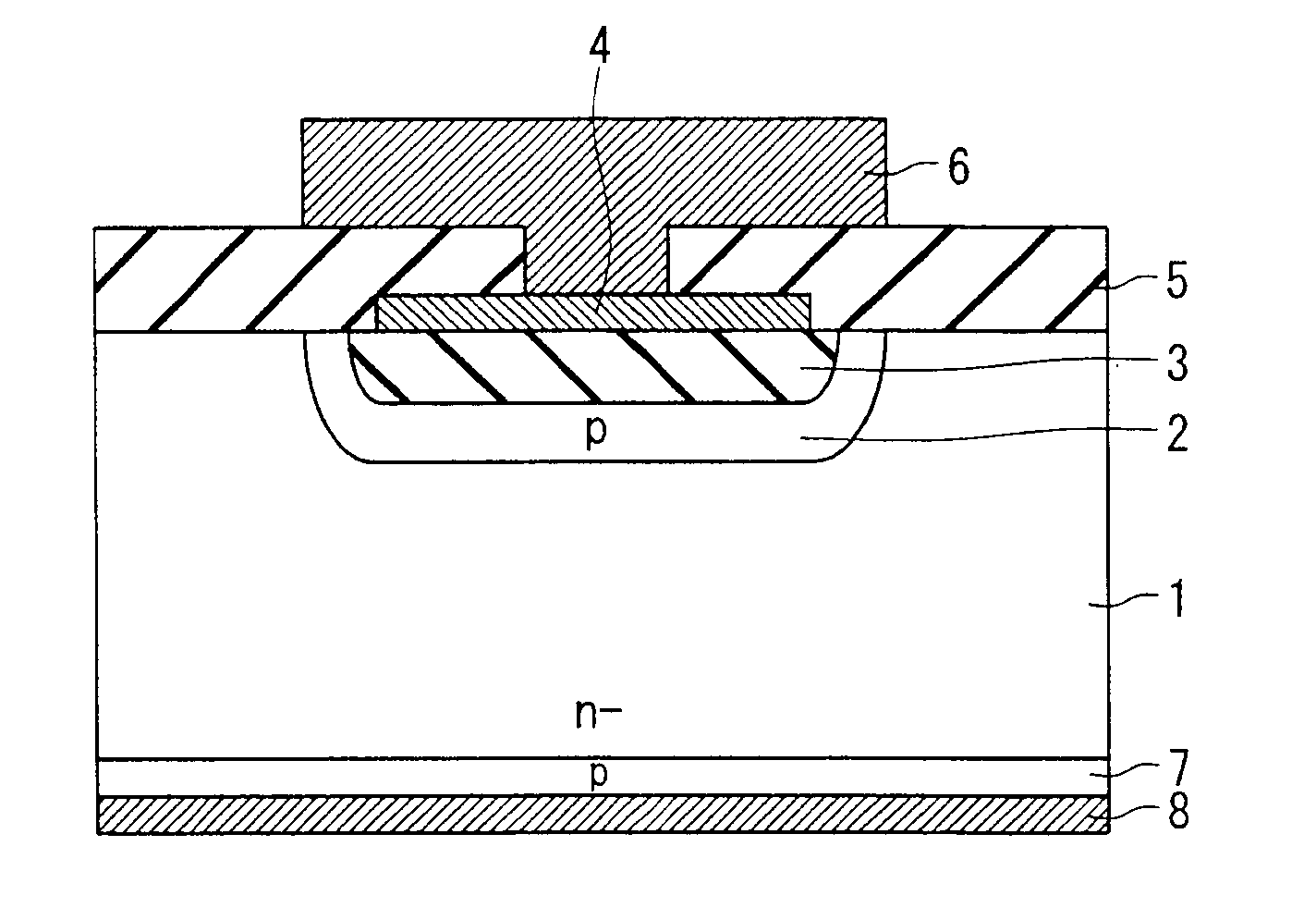
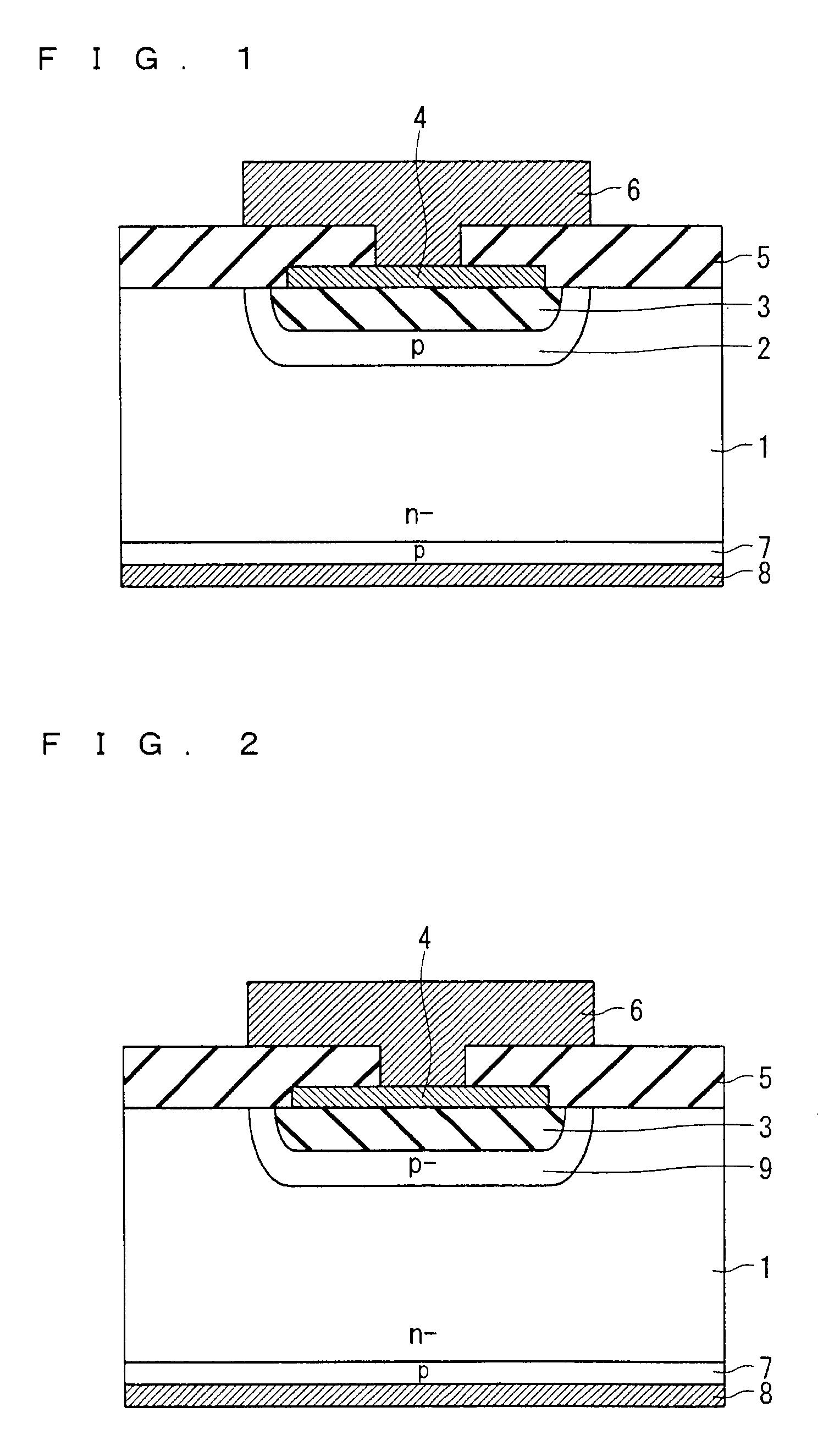
[0031]FIG. 1 is a cross-sectional view showing a configuration of a gate wiring region of a power semiconductor device according to a first preferred embodiment of the present invention. Note that the power semiconductor device according to this preferred embodiment is provided in accordance with a typical chip layout as shown in, for example, FIG. 8, which has a termination region 11 (termination structure) in which a field plate is provided on an insulating film filled in a recessed region (first recessed region) formed in a semiconductor substrate as shown in FIG. 10, and includes a plurality of transistor cell regions 10 (unit cells) connected in parallel. The gate wiring electrically connected to respective gate electrodes of the plurality of transistor cell regions 10 are disposed in a gate wiring region 12, and a gate pad 13 (gate pad region) is electrically connected to the gate wiring region 12.

[0032]As shown in FIG. 1, in the gate wiring region of the power semiconductor d...

second preferred embodiment

[0036]FIG. 2 is a cross-sectional view showing a configuration of a gate wiring region of a power semiconductor device according to a second preferred embodiment of the present invention. As shown in FIG. 2, the second preferred embodiment of the present invention is characterized in that a p-type well region 9 (second impurity region) of low impurity concentration that is formed by ion implantation in which an implantation amount is approximately 1.0E12 atoms / cm2 is provided under the recessed region (second recessed region) formed in the n-type silicon semiconductor substrate 1. Other configuration is similar to that of the first preferred embodiment, and thus description thereof is omitted here.

[0037]In a case where the termination structure is the RESURF structure, a p-type RESURF layer (first impurity region) formed by ion implantation in which an implantation amount is approximately 1.0E12 atoms / cm2 is formed under the recessed region (first recessed region) of the termination...

third preferred embodiment

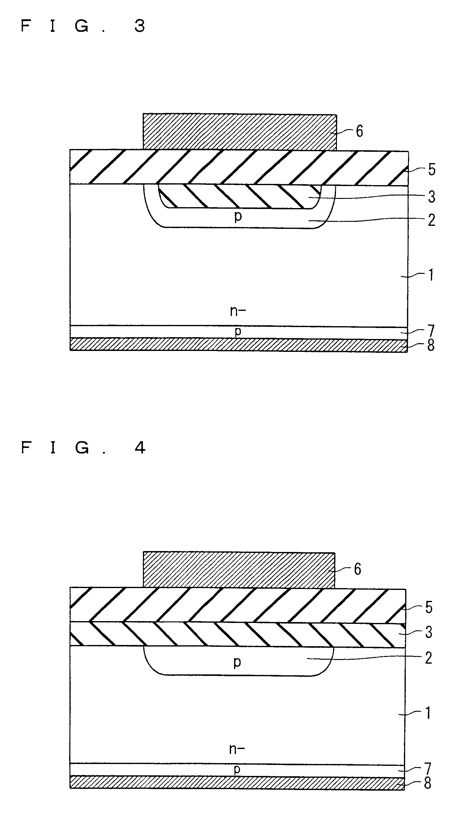
[0039]A third preferred embodiment of the present invention is characterized in that the Al—Si electrode 6 (gate pad region) is disposed above the insulating film 3 filled in a recessed region (third recessed region) formed in the n-type silicon semiconductor substrate 1 (semiconductor substrate).

[0040]FIG. 4 is a cross-sectional view showing a configuration of a gate pad of a conventional power semiconductor device. As shown in FIG. 4, conventionally, the Al—Si electrode 6 (gate pad region) is disposed on the n-type silicon semiconductor substrate 1 through the insulating film 3 and the interlayer film 5. On the Al—Si electrode 6, the gate pad is electrically connected to a gate drive circuit by wire bonding or the like. Conventionally, the thickness of an insulating film formed on the n-type silicon semiconductor substrate 1 is a sum of the thickness of the insulating film 3 and the thickness of the interlayer film 5 as described above, which causes a problem that a step due to th...


PUM

PropertyMeasurementUnit
thicknessaaaaaaaaaa
thicknessaaaaaaaaaa
concentrationaaaaaaaaaa

Abstract

A power semiconductor device according to the present invention, which has a termination structure in which a field plate is provided on an insulating film filled in a recessed region formed in a semiconductor substrate and includes a plurality of unit cells connected in parallel, includes: a gate wiring region in which gate wiring electrically connected to each gate electrode of the plurality of unit cells is provided; and a gate pad region electrically connected to the gate wiring region, wherein the gate wiring region is disposed on the insulating film filled in a recessed region formed in the semiconductor substrate.

Description

BACKGROUND OF THE INVENTION[0001]1. Field of the Invention[0002]The present invention relates to a power semiconductor device, and more particularly, to a power semiconductor device of high breakdown voltage that has a termination structure.[0003]2. Description of the Background Art[0004]In order to relax an electric field at an end of a depletion layer in the vicinity of a main junction surface in a termination of a power semiconductor device of high breakdown voltage such as diodes and bipolar transistors having high breakdown voltage, power metal oxide semiconductor field effect transistors (MOSFETs) and insulated gate bipolar transistors (IGBTs), there is a technology of providing a field plate structure in which a conductive film (field plate) is provided on a semiconductor substrate through an insulating film and providing a reduced surface field (RESURF) layer obtained by selectively providing a low-concentration diffusion layer of conductivity type different from that of the...

Claims


Application Information

Patent Timeline
Patent Type & Authority Patents(United States)
IPC IPC(8): H01L23/58H01L31/0256H01L31/0312H01L29/76H01L29/94H01L31/062H01L31/113H01L31/119
CPCH01L29/0615H01L29/063H01L29/0649H01L29/0661H01L29/402H01L29/4232H01L29/7804H01L29/7811H01L29/0638H01L29/1608H01L29/2003H01L29/7395H01L2924/0002H01L2924/00H01L27/04
Inventor HONDA, SHIGETO
Owner MITSUBISHI ELECTRIC CORP
Why Eureka
Try Eureka