Supercharge Your Innovation With Domain-Expert AI Agents!

Polymer dopants

a technology of polymer and dopants, applied in the field of polymer dopants, can solve the problems of time-dependent mobility and high off curren

Inactive Publication Date: 2013-10-22
MERCK PATENT GMBH
View PDF12 Cites 4 Cited by
  • Summary
  • Abstract
  • Description
  • Claims
  • Application Information

AI Technical Summary

Benefits of technology

The present invention relates to a polymer or a polymer-based material that can be used as a dopant to enhance the charge carrier mobility or electrical conductivity in a semiconductor material. The dopant is a covalently bound electron accepting group that is introduced into the polymer backbone. The invention also includes a novel polymer that can be used as a doping agent in semiconductor materials, such as field effect transistors, charge transport or electroluminescent components in organic light emitting diodes, and sensors. The invention further relates to the use of the polymer or polymer-based material in various electronic devices and components.

Problems solved by technology

A major problem with these small molecule dopants, is that they can be mobile, diffusing through the polymer film or subliming from the surface.
Both these efffects have detrimental consequences for the performance of a working OFET device, potentially leading to time dependant mobility, and high off currents.

Method used


Image

  • Polymer dopants
  • Polymer dopants
  • Polymer dopants

Examples


Embodiment Construction

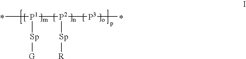
[0040]The polymers according to the present invention are especially suitable as dopant for a semiconductor material in a semiconducting component or device, like for example FETs.

[0041]As the charge transport for example in a FET device occurs mainly at the semiconductor / insulator interface, it is sufficient to only surface dope the semiconductor polymer and still achieve high mobility. This can be achieved by applying a very thin layer of dopant on the semiconductor surface. A further advantage of this approach is that the bulk conductivity remains constant.

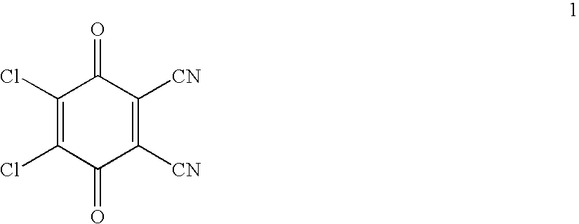
[0042]However, if low molar mass species are used as dopants, a problem associated with this approach is that the dopant can diffuse throughout the transistor structure, or sublime from the surface, both reducing the surface effect, and potentially disrupting morphology and hence mobility. This problem is circumvented according to the present invention by anchoring the dopant as a polymer component, thus eliminating diffusion o...


PUM

PropertyMeasurementUnit
frequenciesaaaaaaaaaa
frequencyaaaaaaaaaa
depositionaaaaaaaaaa

Abstract

A polymer dopant for electrially conducting, photoconducting and semiconducting components and devices and novel polymers comprising electron accepting groups that are suitable as polymer dopants.

Description

[0001]This application is a continuation of U.S. application Ser. No. 10 / 763,382 filed Jan. 26, 2004 now U.S. Pat. No. 7,186,358 claiming the benefit of European application number 03001678.6 filed Jan. 25, 2003.FIELD OF INVENTION[0002]The invention relates to the use of polymer dopants for electrically conducting, photoconducting and semiconducting components and devices and to novel polymers comprising electron accepting groups that are suitable as polymer dopants.BACKGROUND AND PRIOR ART[0003]In the field of organic semiconductors, a major effort exists to improve the charge carrier mobility of the organic semiconductor material to levels approaching amorphous silicon (0.1 cm2 / Vs) [see H. E. Katz, Z. Bao and S. L. Gilat, Acc. Chem. Res., 2001, 34, 5, 359]. This would enable organic field effect transistors (OFET) to operate at frequencies that make them attractive for a host of applications including radio frequency identification (RFID) tags and thin film transistors (TFT) in fl...

Claims


Application Information

Patent Timeline
Patent Type & Authority Patents(United States)
IPC IPC(8): H01B1/06H01L51/50H01B1/12H01L29/786H01L33/00H01L33/26H01L51/05H01L51/30H01L51/40
CPCH01L51/002H01L51/004H01L51/0051H01L51/0052H01L51/0067H01L51/007Y02E10/549H10K71/30H10K85/141H10K85/611H10K85/615H10K85/6565H10K85/654
Inventor MCCULLOCH, IAINHEENEY, MARTINGILES, MARKSHKUNOV, MAXIMTIERNEY, STEVENBAILEY, CLARE
Owner MERCK PATENT GMBH
Features
  • R&D
  • Intellectual Property
  • Life Sciences
  • Materials
  • Tech Scout
  • Unparalleled Data Quality
  • Higher Quality Content
  • 60% Fewer Hallucinations
Learn More