
Laser crystallization apparatus and laser crystallization method using the same

a laser crystallization and crystallization device technology, applied in the direction of optical resonator shape and construction, manufacturing tools, welding/soldering/cutting articles, etc., can solve the problem of linear error portion, undesirable non-uniformity of polycrystalline silicon, and limitation in removing a dot pattern defect, so as to reduce the display error of the dot pattern and improve the uniformity

Active Publication Date: 2013-11-19
SAMSUNG DISPLAY CO LTD
View PDF13 Cites 0 Cited by
  • Summary
  • Abstract
  • Description
  • Claims
  • Application Information

AI Technical Summary

Benefits of technology

The present invention is about a device and method for laser crystallization that reduces display error and non-uniformity in polycrystalline silicon production. It does this by calculating the vibration frequency of the laser beam and minimizing the regions where multiple pulses overlap constructively. This results in a more uniform display and improved device manufacturing.

Problems solved by technology

At this time, if the laser beam profile as the linear pattern may have an error portion, a linear error portion may be generated along a scan direction of the laser.
By irradiating the vibrating laser beam onto the amorphous silicon thin film, however, there is a limitation in removing a defect of a dot pattern.
This dot pattern inhomogeneity in the laser beam profile may cause undesirable nonuniformities in the polycrystalline silicon.

Method used


Image

  • Laser crystallization apparatus and laser crystallization method using the same
  • Laser crystallization apparatus and laser crystallization method using the same
  • Laser crystallization apparatus and laser crystallization method using the same

Examples


Embodiment Construction

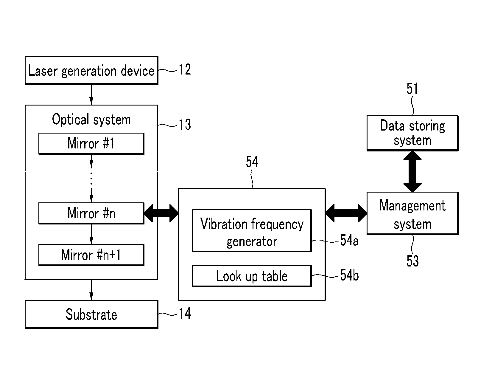
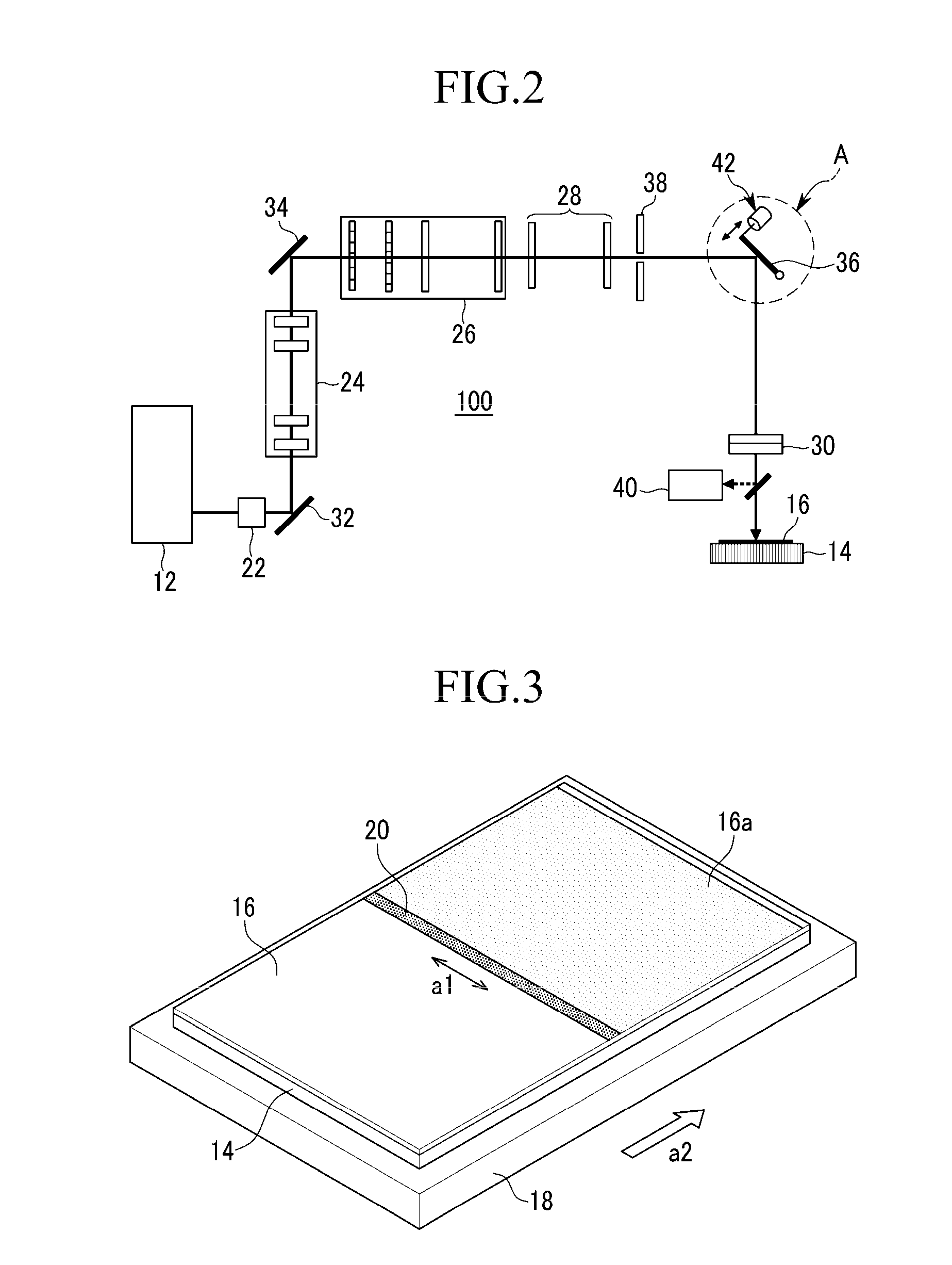
[0055]Exemplary embodiments of the present invention are described in detail with reference to the accompanying drawings. The present invention is not limited to exemplary embodiments described herein, however, but may be embodied in other forms. As one example, optics in the schematic diagrams may often be replaced with their reflective, refractive, or diffractive counterparts to give a similar result. Rather, exemplary embodiments described herein are provided to thoroughly and completely understand the disclosed contents and to sufficiently transfer the ideas of the present invention to a person of ordinary skill in the art.

[0056]In the drawings, the thickness of layers and regions are exaggerated for clarity. It is to be noted that when a layer is referred to as being “on” another layer or substrate, it can be directly formed on another layer or substrate or can be formed on another layer or substrate through an intervening third layer. Like constituent elements are denoted by l...


PUM

PropertyMeasurementUnit
vibration frequencyaaaaaaaaaa
speedaaaaaaaaaa
electrical mobilityaaaaaaaaaa

Abstract

A laser crystallization device is provided, which includes a vibration device vibrating a laser beam along its long axis, wherein a vibration frequency at which the laser beam vibrates is satisfied by Equation 1 below.F<(P*f) / (2*W)  Equation 1where F is the mirror vibration frequency, W is the laser beam width, P is the laser scan pitch, and f is the laser pulse frequency.

Description

CROSS-REFERENCE TO RELATED APPLICATION[0001]This application claims priority to and the benefit of Korean Patent Application No. 10-2011-0105326 filed in the Korean Intellectual Property Office on Oct. 14, 2011, the entire contents of which are incorporated herein by reference.BACKGROUND OF THE INVENTION[0002](a) Field of the Invention[0003]The present invention relates to a laser crystallization device and a laser crystallization method.[0004](b) Description of the Related Art[0005]Both liquid crystal displays (LCDs) and organic light emitting diode (OLED) displays can be fabricated to be thin and lightweight. These types of flat panel display devices are commonly used as displays in mobile electronic devices, and their application coverage extends to large-scale display devices. As the necessity for display devices requiring high speed operational characteristics emerges, research on such a display device is actively ongoing.[0006]To satisfy the high speed operational characterist...

Claims


Application Information

Patent Timeline
Patent Type & Authority Patents(United States)
IPC IPC(8): H01S3/121H01S3/10H01S3/08
CPCH01L21/02691B23K26/0042B23K26/0643H01L21/02532H01L21/02678H01L21/02686B23K26/0006B23K2103/56B23K26/0738H01L21/02675H01L27/1285
Inventor OKUMURA, HIROSHI
Owner SAMSUNG DISPLAY CO LTD
Learn More