Organic light-emitting panel for controlling an organic light emitting layer thickness and organic display device

a light-emitting panel and organic technology, applied in the direction of electroluminescent light sources, thermoelectric devices, electric lighting sources, etc., can solve the problem of uneven film thickness of organic light-emitting layers, and achieve excellent light-emitting characteristics, prevent uneven film thickness, and prevent uneven film thickness

Active Publication Date: 2013-12-10
JOLED INC
View PDF64 Cites 5 Cited by
  • Summary
  • Abstract
  • Description
  • Claims
  • Application Information

AI Technical Summary

Benefits of technology

[0018]The organic light-emitting panel according to the above aspect of the present invention has the structure that, with respect to two opposing banks defining the third light-emitting cell of the first pixel, an inclination angle of a wall facing the third light-emitting cell of the first pixel in the first bank located closer to the non-light-emitting cell is larger than an inclination angle of a wall facing the third light-emitting cell of the first pixel in the bank located closer to the second light-emitting cell. With the above structure, with respect to the two opposing banks defining the third light-emitting cell of the first pixel when ink for forming an organic light-emitting layer is dripping, the height of a pinning location of the ink in a wall facing the third light-emitting cell of the first pixel in the first bank located closer to the non-light-emitting cell becomes higher than a pinning location of the ink in a wall facing the third light-emitting cell of the first pixel in the bank located closer to the second light-emitting cell. By making the pinning location high as mentioned above, the organic light-emitting panel according to the aspect of the present invention is capable of preventing uneven film thickness in the third light-emitting cell of the first pixel of the organic light-emitting layer, despite the fact that the film thickness of a section in the third light-emitting cell of the first pixel adjacent to the first bank tends to become relatively thick due to non-uniform vapor concentration distribution when the ink for forming the organic light-emitting layer is dripping.
[0019]The organic light-emitting panel according to the aspect of the present invention also has the structure that, with respect to two opposing banks defining the first light-emitting cell of the second pixel, an inclination angle of a wall facing the first light-emitting cell of the second pixel in the second bank located closer to the non-light-emitting cell is larger than an inclination angle of a wall facing the first light-emitting cell of the second pixel in the bank located closer to the second light-emitting cell. With the above structure, with respect to the two opposing banks defining the first light-emitting cell of the second pixel when the ink for forming an organic light-emitting layer is dripping, the height of a pinning location of the ink in the wall facing the first light-emitting cell of the second pixel in the second bank located closer to the non-light-emitting cell becomes higher than a pinning location of the ink in the wall facing the first light-emitting cell of the second pixel in the bank located closer to the second light-emitting cell. By making the pinning location high as mentioned above, the organic light-emitting panel according to the aspect of the present invention is capable of preventing uneven film thickness in the first light-emitting cell of the second pixel of the organic light-emitting layer, despite the fact that the film thickness of a section in the first light-emitting cell of the second pixel adjacent to the second bank tends to become relatively thick due to the non-uniform vapor concentration distribution when the ink for forming the organic light-emitting layer is dripping.
[0020]Note that although the non-light-emitting cell is provided between the third light-emitting cell of the first pixel and the first light-emitting cell of the second pixel, ink for forming the organic light-emitting layer is not applied to the non-light-emitting cell. For this reason, in the section in the third light-emitting cell of the first pixel adjacent to the first bank and in the section in the first light-emitting cell of the second pixel adjacent to the second bank, the vapor concentration tends to become relatively low in comparison with other sections in these light-emitting cells of the first and the second pixel remote from the first and the second bank due to the presence of the non-light-emitting cell in which ink is not dripping, whereby the film thickness of the organic light-emitting layer tends to be thick in these sections. In view of the above tendencies, the aspect of the present invention prevents uneven film thickness of the organic light-emitting layer in the third light-emitting cell of the first pixel and in the first light-emitting cell of the second pixel, by setting the inclination angles of the bank walls to have the above relationships.
[0021]As a result, the organic light-emitting panel according to the aspect of the present invention prevents uneven film thickness in the organic light-emitting layer both in the third light-emitting cell of the first pixel and in the first light-emitting cell of the second pixel on either side of the non-light-emitting cell, which allows for excellent light-emitting characteristics to be obtained.

Problems solved by technology

However, it is problematic to even out the film thickness of the organic light-emitting layer formed in this way.

Method used


Image

  • Organic light-emitting panel for controlling an organic light emitting layer thickness and organic display device
  • Organic light-emitting panel for controlling an organic light emitting layer thickness and organic display device
  • Organic light-emitting panel for controlling an organic light emitting layer thickness and organic display device

Examples


embodiment

[Embodiment]

[0094]The following describes an example of an embodiment of the present invention with reference to the drawings.

[0095]Note that the following Embodiment is simply an example to clearly illustrate a structure of the present invention and the effects and advantages thereof. The present invention is in no way limited to the following Embodiment except in its essential characteristic elements.

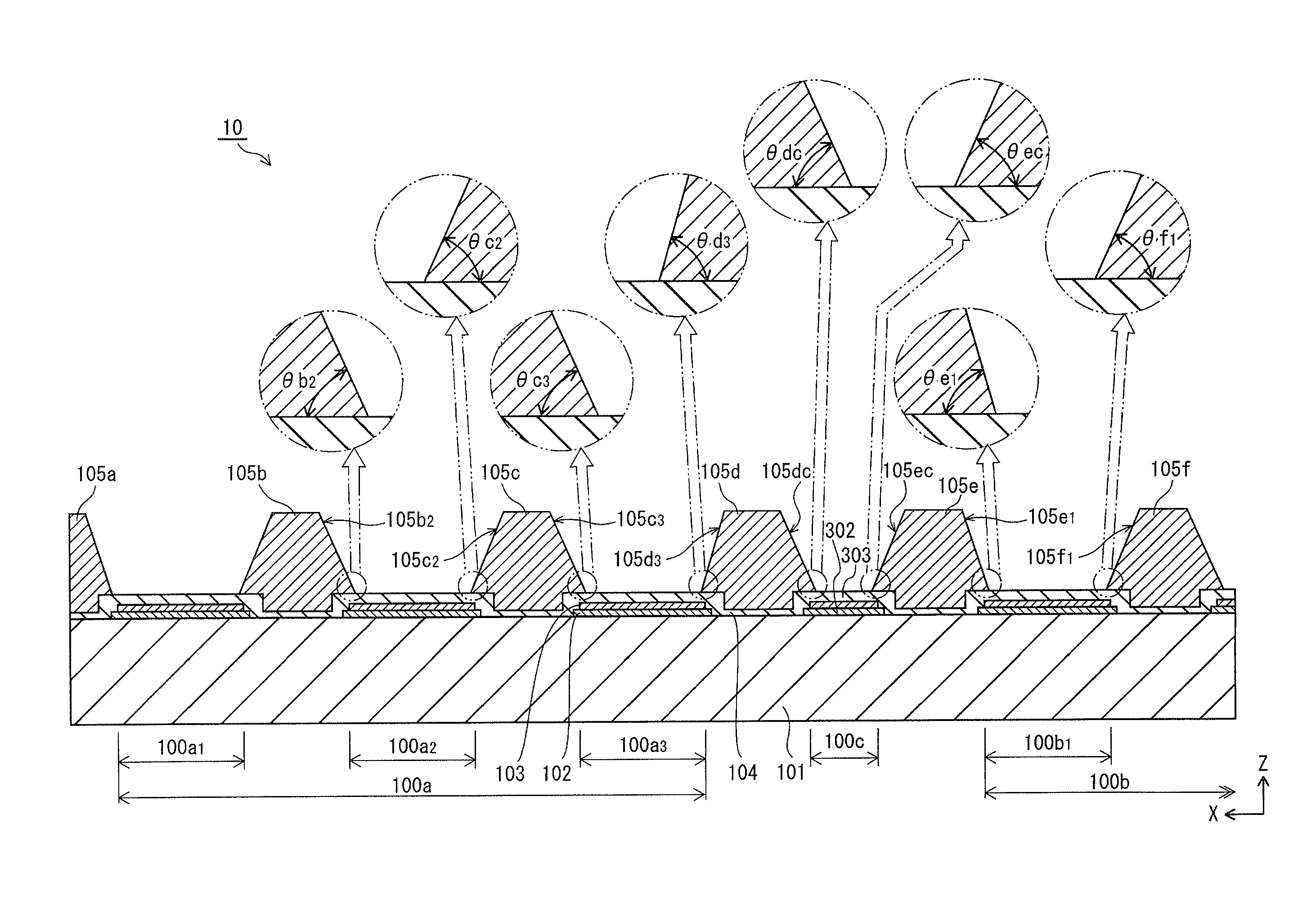
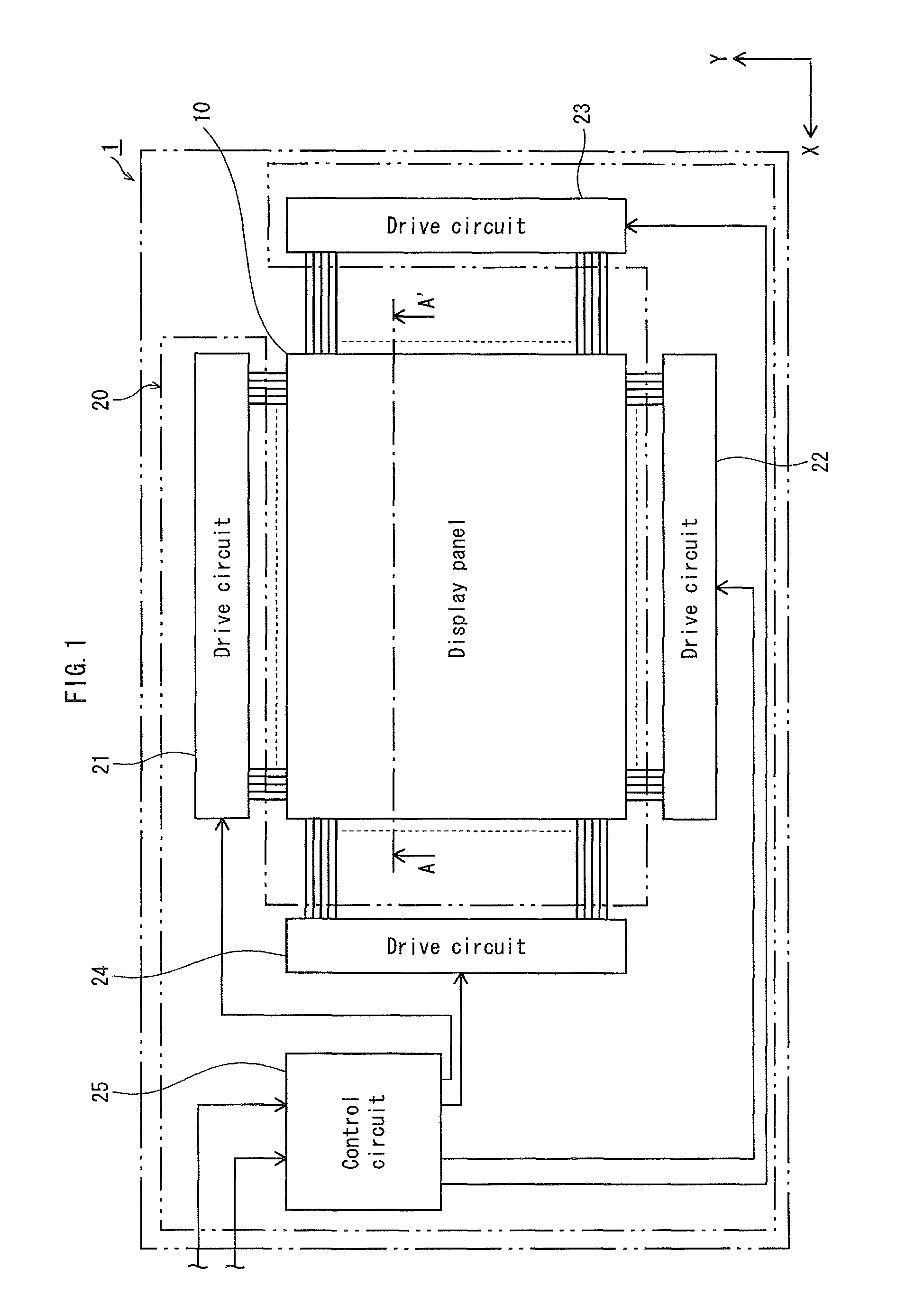
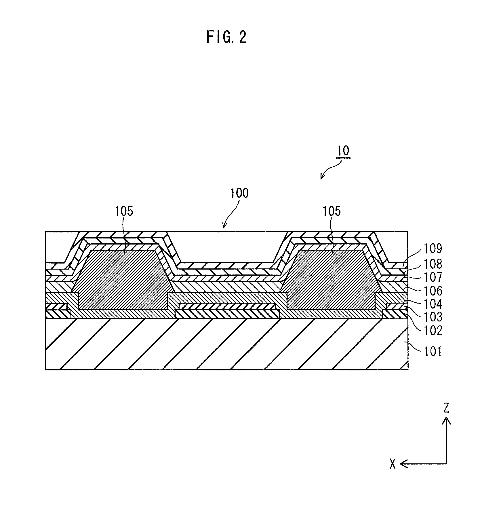
[0096]1. Configuration of Display Device 1

[0097]The overall structure of the display device 1 according to the present Embodiment is described with reference to FIG. 1.

[0098]As shown in FIG. 1, the display device (organic display device) 1 includes a display panel unit 10 and a drive control unit 20 connected to the display panel unit 10. The display panel unit 10 is an organic EL panel that uses the phenomenon of electroluminescence occurring in organic material and is composed of an array of a plurality of pixels arranged two-dimensionally in X and Y directions.

[0099]The drive contr...

modification 1

[Modification 1]

[0176]Next, with reference to FIG. 12, Modification 1 of the manufacturing method of the display device 1 is described. FIG. 12 shows processes corresponding to the processes shown from FIGS. 9C-10A.

[0177]As shown in FIG. 12, after layering the bank material layer 1050 on top of the hole injection transporting layer 104, a mask 503 is placed above the bank material layer 1050. The mask 503 has optical transmission sections 503a, 503b1, 503b2, 503c1, and 503c2. The optical transmission section 503a is provided in correspondence to the location where the bank 105c is to be formed, the optical transmission sections 503b1 and 503b2 are provided in correspondence to the location where the bank 105d is to be formed, and the optical transmission sections 503c1 and 503c2 are provided in correspondence to the location where the bank 105e is to be formed.

[0178]In the manufacturing method of the display device 1 according to Modification 1, the width We of the optical transmiss...

modification 2

[Modification 2]

[0184]Next, with reference to FIGS. 13 and 14, Modification 2 of the manufacturing method of the display device 1 is described. FIGS. 13 and 14 show processes corresponding to the processes shown from FIGS. 9C-10B.

[0185]As shown in FIG. 13A, after layering the bank material layer 1050 on top of the hole injection transporting layer 104, a mask 504 is placed above the bank material layer 1050. The mask 504 has openings 504a, 504b, and 504c which are provided in correspondence to the locations where the banks 105 are to be formed.

[0186]The opening 504a is formed to have the same width as the opening 501a in the mask 501 used in the manufacturing method of the above Embodiment.

[0187]On the other hand, the width Wd3 (We3) of the opening 504b (504c) provided in the location between the region 1000a3 in which the sub-pixel is to be formed and the region 1000c in which the non-light-emitting cell is to be formed (between the region 1000b1 in which the sub-pixel is to be for...


PUM


Abstract

A non-light-emitting cell 100c is provided between pixels 100a and 100b. Ink for forming an organic light-emitting layer is dripped substantially simultaneously into sub-pixels 100a1, 100a2, and 100a3 in the pixel 100a and a sub-pixel 100b1 in the pixel 100b. On the other hand, such ink is not dripped into the non-light-emitting cell 100c since the organic light-emitting layer is not formed in the non-light-emitting cell 100c. Regarding two banks 105c and 105d defining the sub-pixel 100a3, an inclination angle θd3 of a wall 105d3 of the bank 105d is larger than an inclination angle θc3 of a wall 105c3 of the bank 105c. Similarly, regarding banks 105e and 105f defining the sub-pixel 100b1, an inclination angle θe1 of a wall 105e1 of the bank 105e is larger than an inclination angle θf1 of a wall 105f1 of the bank 105f.

Description

CROSS REFERENCE TO RELATED APPLICATION[0001]This is a continuation application of PCT Application No. PCT / JP2010 / 006144 filed on Oct. 15, 2010, designating the United States of America, the disclosure of which, including the specification, drawings and claims, is incorporated herein by reference in its entirety.TECHNICAL FIELD[0002]The present invention relates to an organic light-emitting panel and a manufacturing method thereof, and an organic display device.BACKGROUND ART[0003]In recent years, progress has been made in the research and development of display devices that use the phenomenon of electroluminescence occurring in organic material. Each pixel of such a display device is composed of an anode and a cathode with an organic light-emitting layer therebetween. For driving the display device, holes are injected through the anode and electrons are injected through the cathode. Then, holes and electrons recombine in the organic light-emitting layer, and light is emitted.[0004]B...

Claims


Application Information

Patent Timeline
Patent Type & Authority Patents(United States)
IPC IPC(8): H01L29/18H01L21/00H01L29/08H01L33/00H01L29/20
CPCH01L27/3211H01L27/3223H05B33/10H01L27/3246H01L51/0005H10K59/88H10K59/35H10K71/135H10K59/122H10K10/46
Inventor MATSUSHIMA, HIDEAKI
Owner JOLED INC
Why Eureka
Try Eureka