Method for fabricating high-gain MOSFETs with asymmetric source/drain doping for analog and RF applications

a technology of asymmetric source/drain and mosfet, which is applied in the direction of transistors, electrical devices, semiconductor devices, etc., can solve the problems of serious limitation of analog applications, long gates may not exhibit higher gains, and anomalous high output conductance of analog fets, so as to reduce junction leakage and reduce output resistance

Inactive Publication Date: 2014-01-21
IBM CORP
View PDF8 Cites 7 Cited by
  • Summary
  • Abstract
  • Description
  • Claims
  • Application Information

AI Technical Summary

Benefits of technology

[0019]HALO implant—The term HALO implant may denote a special doped area adjacent to the gate. The source-to-substrate and drain-to-substrate junctions of a FET may be an object of much attention in the design of the FET because of three major factors: the design may affect the current-voltage characteristics of the device, it may lower an output resistance, and also influence the speed or frequency characteristics of the device through the loading effect of junction capacitances, and finally, the component of stand-by power dissipation, due to junction leakage may be reduced.
[0021]Extension implant—The term extension implant area may denote areas which may typically be just below the gate on both sides of the gate. On one side, a source side extension may reach into a source area. On the other side, a drain side extension area may reach into a drain area. The extension areas—also junction extensions—have a positive effect on a drain induced barrier lowering of the threshold voltage and channel length modulation effects upon I-V curves.

Problems solved by technology

Typically used HALO implants—also known as pocket implants—may induce potential drain-side barriers that result in anomalously high output conductance of analog FETs (field effect transistor).
Thus, longer gates may not exhibit higher gains.
This may be a serious limitation for analog applications that may also require SRAM cells as well as other logic gates on the same substrate.

Method used


Image

  • Method for fabricating high-gain MOSFETs with asymmetric source/drain doping for analog and RF applications
  • Method for fabricating high-gain MOSFETs with asymmetric source/drain doping for analog and RF applications
  • Method for fabricating high-gain MOSFETs with asymmetric source/drain doping for analog and RF applications

Examples


Embodiment Construction

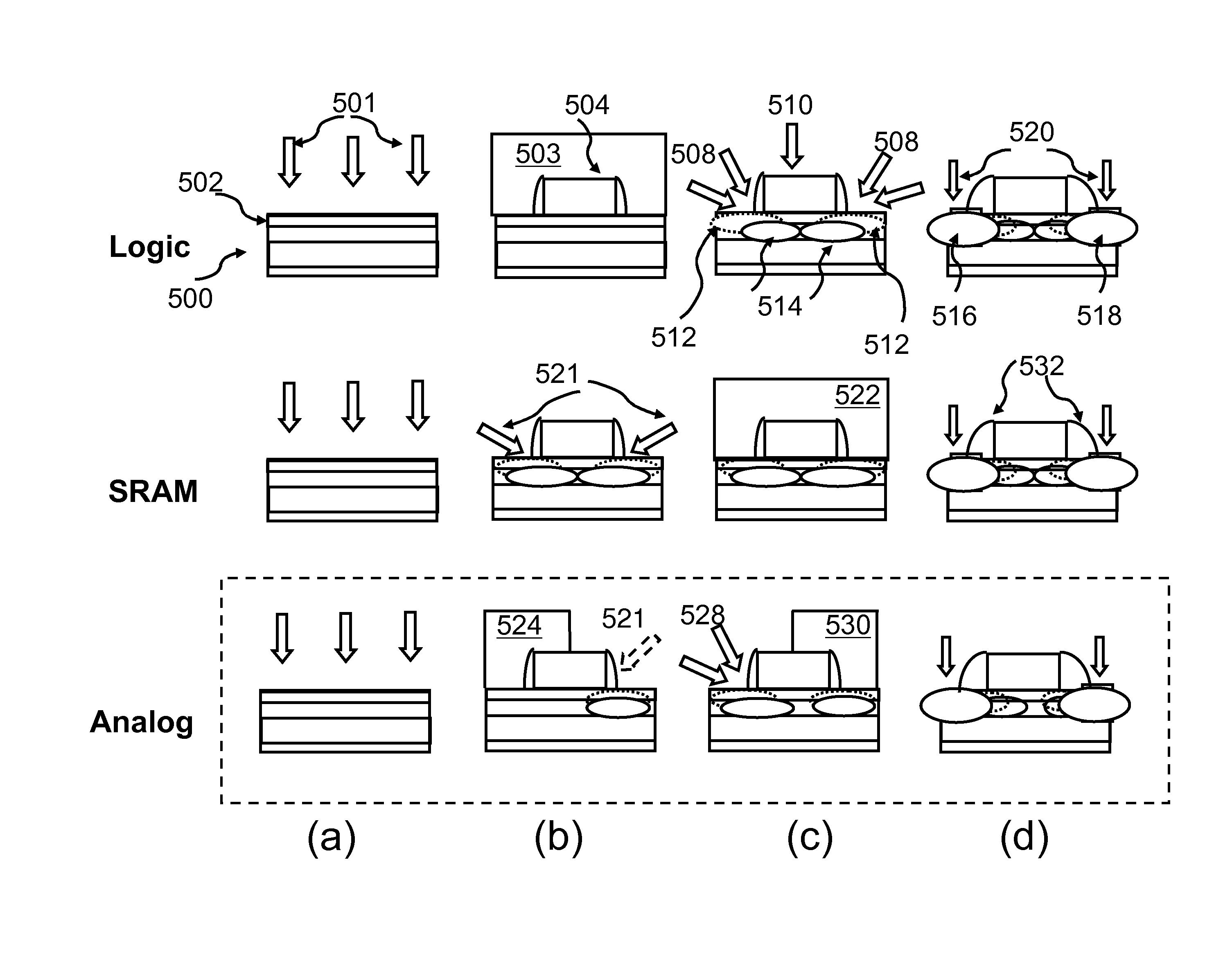
[0033]A detailed description of the figures now follows. All illustrations in the figures are schematic.

[0034]It should be noted that embodiments of the invention are described with reference to particular subject-matters, such as with reference to method type claims, whereas other embodiments have been described with reference to apparatus type claims. However, a person skilled in the art will gather from the above and the following description that, unless otherwise notified, in addition to any combination of features belonging to one type of subject-matter, also any combination between features relating to different subject-matters, in particular between features of the method type claims, and features of the apparatus type claims, is considered as to be disclosed within this document.

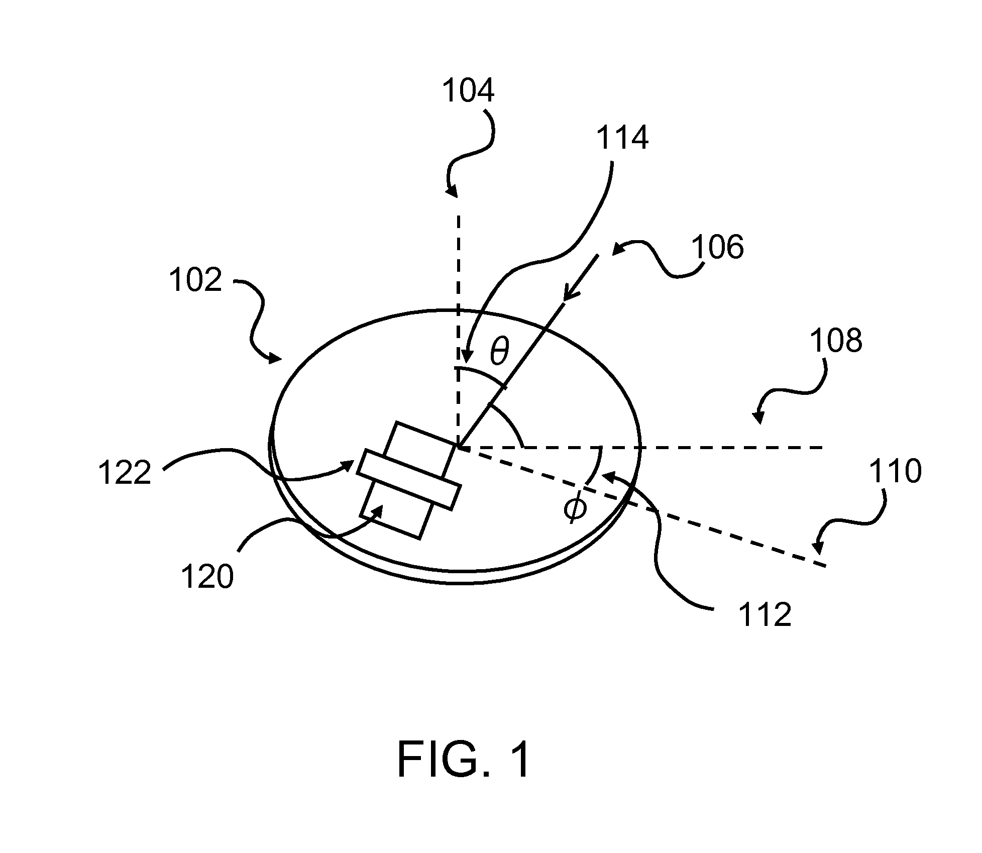
[0035]FIG. 1 illustrates a conventional spatial orientation diagram used for angled implants. A substrate 102 can be a silicon wafer. The wafer or substrate may be covered with a dielectric. Arrow 1...


PUM


Abstract

A method of fabrication of an analog, asymmetric Metal-Oxide-Semiconductor-Field-Effect-Transistor (MOSFET) is provided. The method may comprise forming a first gate oriented in a first direction over an active region of a semiconductor substrate, forming a second gate extending perpendicular to the first gate over a second active region, using a dual-directional implant process to form a reduced-HALO doped area on a drain side of the first gate and also for a HALO doped area for the second gate, while the source side of the first gate is covered by a resist. Additionally, the method may comprise forming a HALO doped area on the source side of the first gate using a quad-directional implant process using the mask also used for HALO implants of other digital-logic devices on the substrate, while the drain side of the gate is blocked by a resist.

Description

FIELD OF THE INVENTION[0001]The invention relates generally to a method for fabricating of an analog, asymmetric Metal-Oxide-Semiconductor-Field-Effect-Transistor (MOSFET). In particular, the invention relates to a method of fabricating logic devices, SRAM cells and analog MOSFETs with a reduced set of masks. Additionally, the invention relates to a system adapted to implement the method.BACKGROUND OF THE INVENTION[0002]Structures of semiconductor devices are becoming smaller and smaller. On one side, there are logic devices, e.g., NAND or NOR gates, and storage devices like SRAM cells (static random access memory). On the other side, there are analog devices. In many cases, it may be required to combine the different types of devices on a single substrate. However, the device characteristics and consequently the fabrication requirements may differ significantly. For example, there may always be a requirement for high gain coefficients of analog transistors.[0003]Typically used HALO...

Claims


Application Information

Patent Timeline
Patent Type & Authority Patents(United States)
IPC IPC(8): H01L21/336H01L21/8238
CPCH01L21/26586H01L29/66772H01L27/1104H01L29/66659H01L29/1083H01L27/105H10B10/12
Inventor LASSERRE, SEBASTIENPEKARIK, JOHN J.
Owner IBM CORP
Why Eureka
Try Eureka