

Compact folded configuration for integrated circuit packaging
a technology of integrated circuit and folding configuration, which is applied in the direction of instruments, cross-talk/noise/interference reduction, and the details of semiconductor/solid-state devices, to achieve the effect of thin and lighter weight design
- Summary
- Abstract
- Description
- Claims
- Application Information
AI Technical Summary
Benefits of technology
Problems solved by technology
Method used
Image

Examples
Embodiment Construction
[0029]In the following detailed description, numerous specific details are set forth to provide a thorough understanding of the concepts underlying the described embodiments. It will be apparent, however, to one skilled in the art that the described embodiments can be practiced without some or all of these specific details. In other instances, well known process steps have not been described in detail in order to avoid unnecessarily obscuring the underlying concepts.
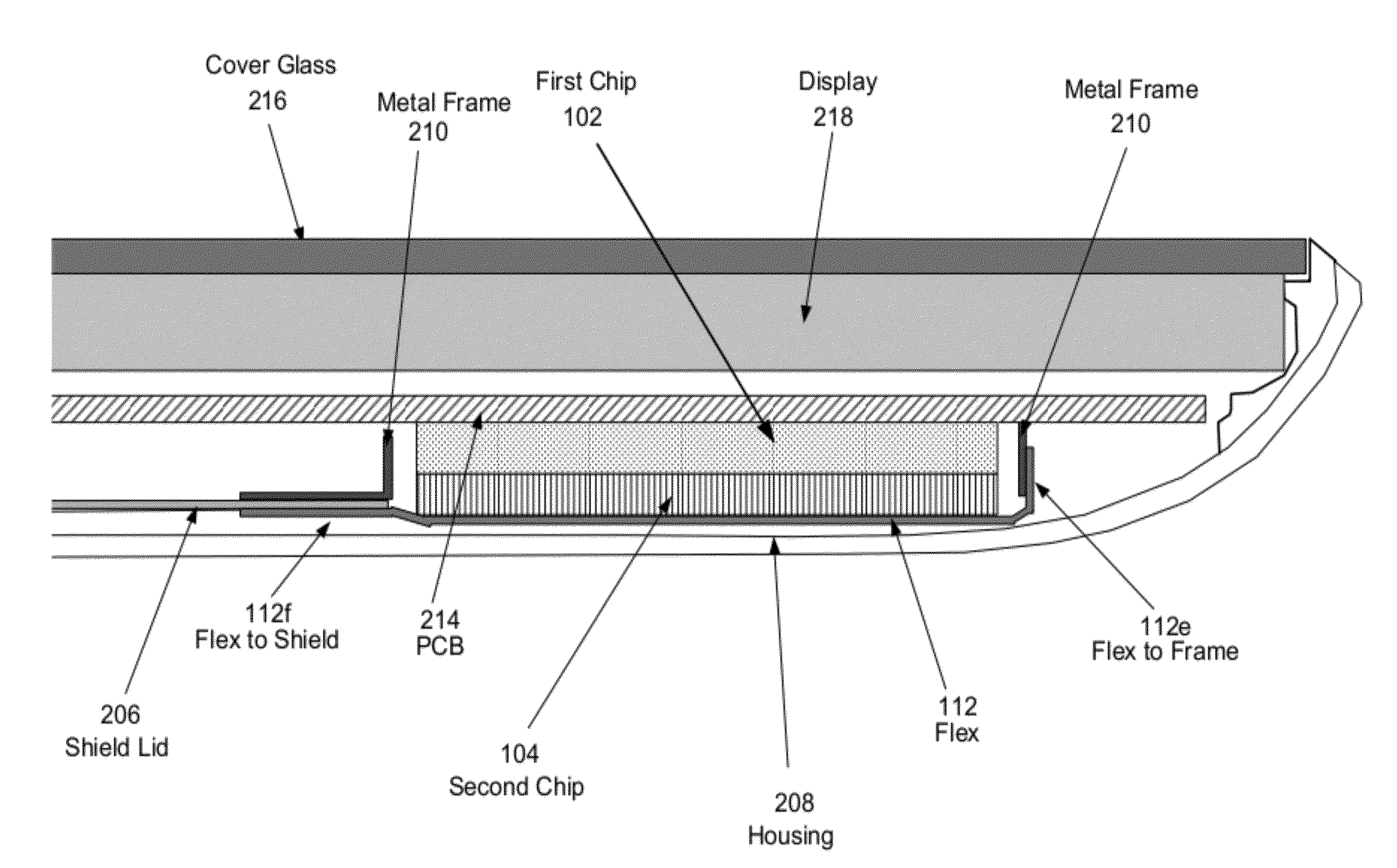
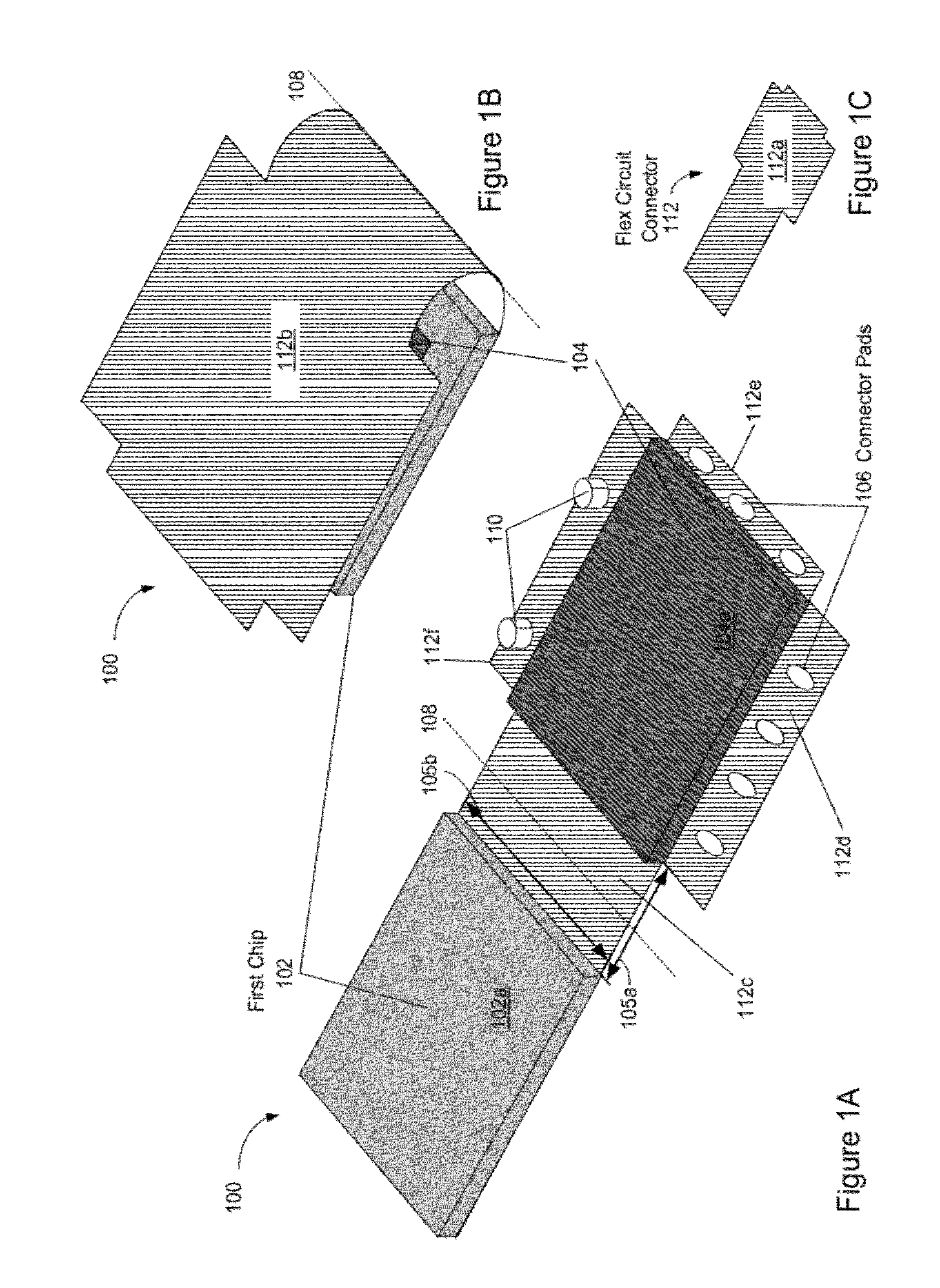
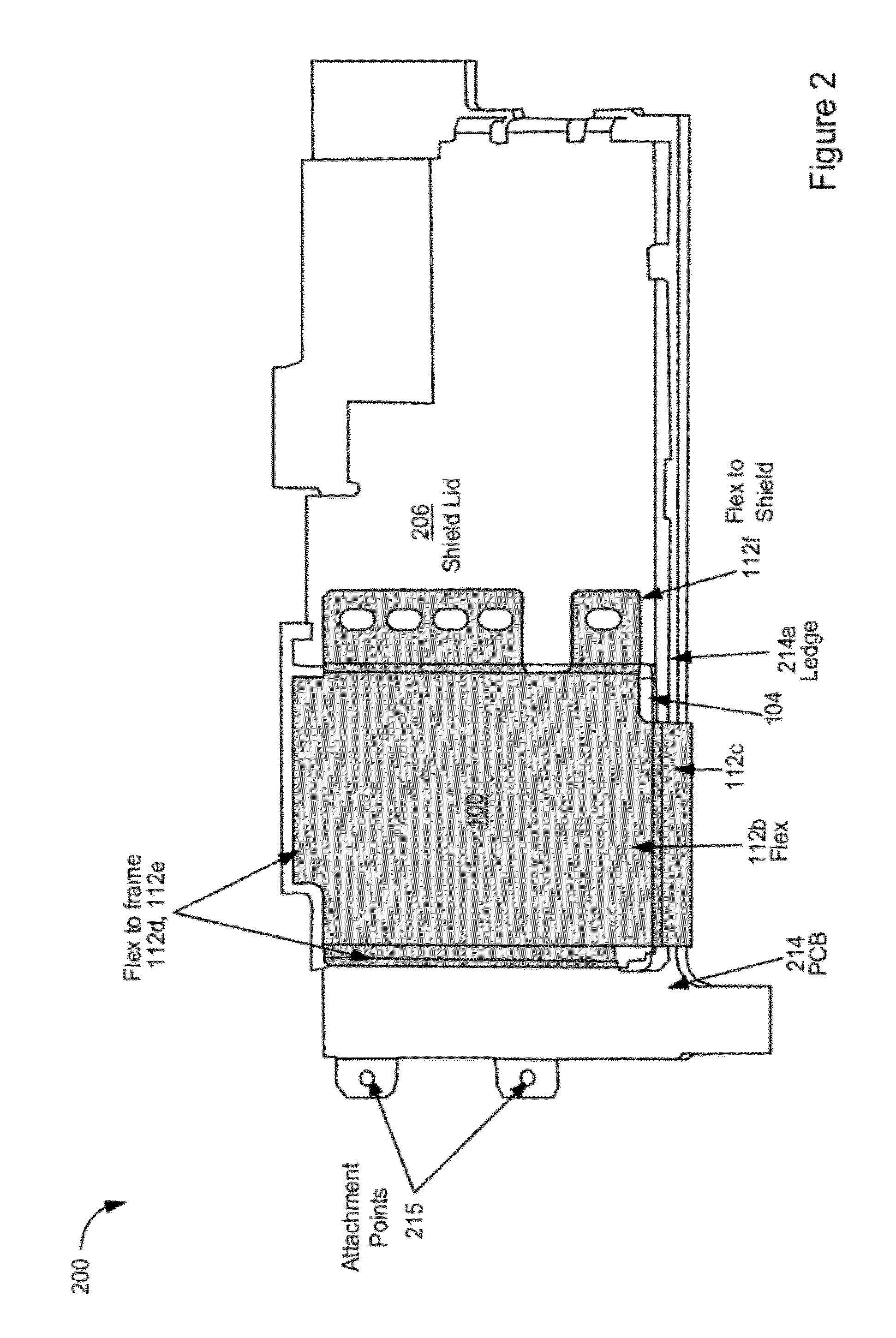
[0030]Broadly speaking, the embodiments disclosed herein relate to compact form factor integrated circuit packaging designs well suited for use in portable computing devices. For the remainder of this discussion and without loss of generality, the integrated circuits will be discussed in terms of memory devices such as FLASH memory devices, In particular, the FLASH memory devices can take the form of NAND type memory devices widely used in portable computing devices. The packaging designs take into consideration factors ...
PUM
| Property | Measurement | Unit |
|---|---|---|
| flexible | aaaaa | aaaaa |
| radio frequency | aaaaa | aaaaa |
| conductive | aaaaa | aaaaa |
Abstract
Description
Claims
Application Information