Wireless communication device
a communication device and wireless technology, applied in the direction of instruments, substantially flat resonant elements, resonant antennas, etc., can solve the problems of reducing communication range and reducing the work of antennas, and achieve the effect of broadening the operating frequency band
- Summary
- Abstract
- Description
- Claims
- Application Information
AI Technical Summary
Benefits of technology
Problems solved by technology
Method used
Image

Examples
first embodiment
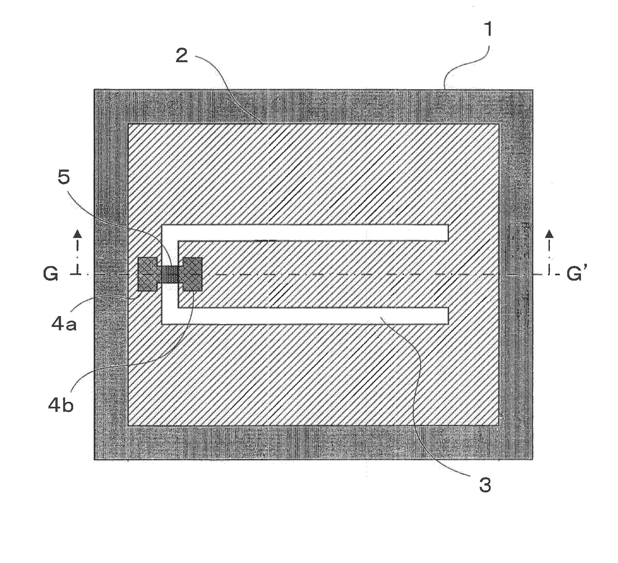
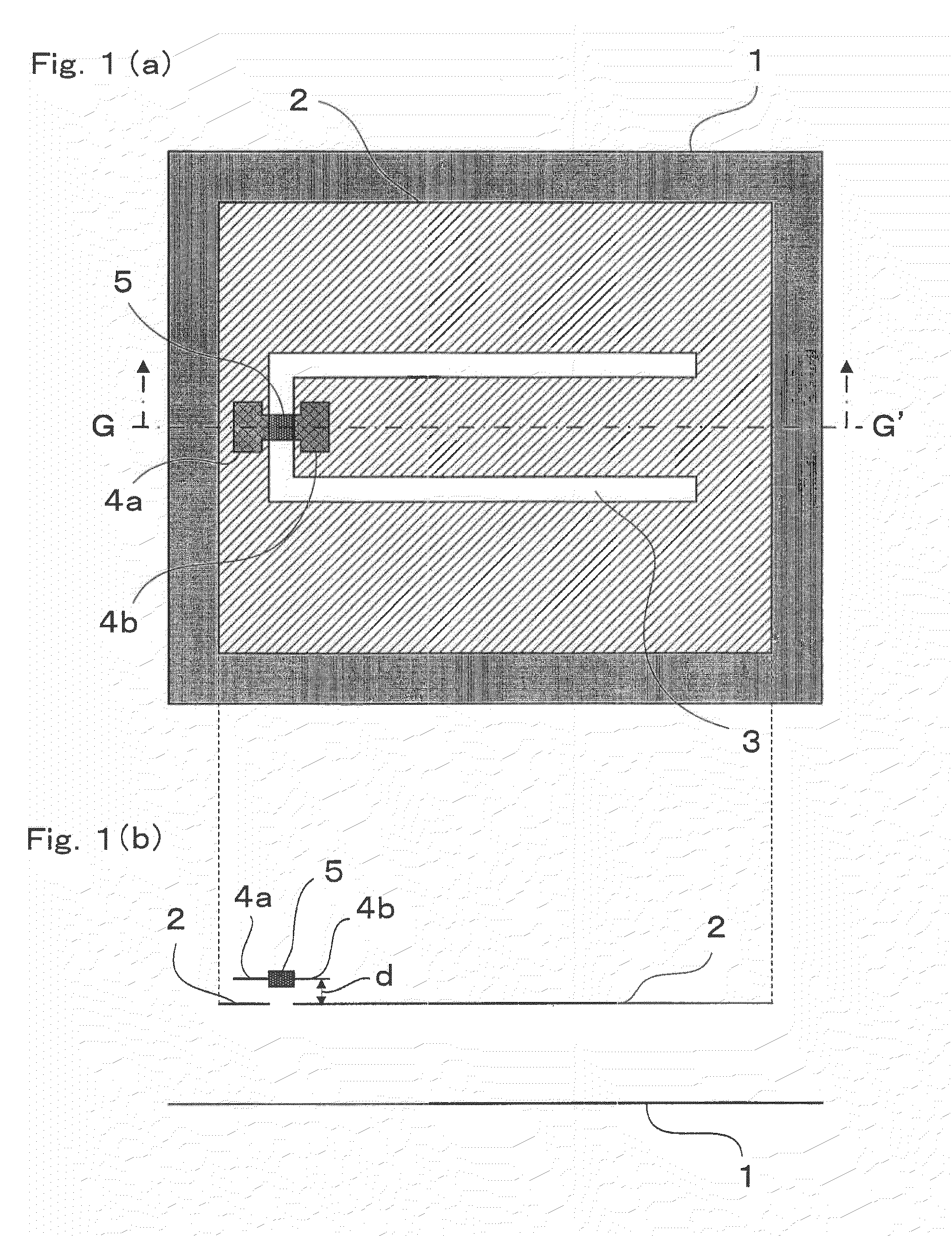
[0033]FIG. 1 are a plan view and a sectional view illustrating a wireless communication device according to a first embodiment of the present invention, and illustrate the structure of an RFID tag which functions as a wireless communication device.
[0034]FIG. 1(a) is a plan view, and FIG. 1(b) is a sectional view taken along the line G-G′ of FIG. 1(a).
[0035]In FIG. 1, the RFID tag includes a ground conductor 1, a radiation conductor (hereinafter, simply referred to as “conductor”) 2, a slot line (hereinafter, simply referred to as “slot”) 3, capacitive coupling means 4a and 4b, and an IC chip 5.
[0036]The ground conductor 1 is a conductor of a finite size and has, for example, a rectangular shape as illustrated in FIG. 1(a). The conductor 2 is a plate-like conductor and has, for example, a rectangular shape as the ground conductor 1 does.
[0037]The conductor 2 is disposed substantially parallel to the ground conductor 1 with a gap therebetween, and constitutes together with the ground ...
second embodiment
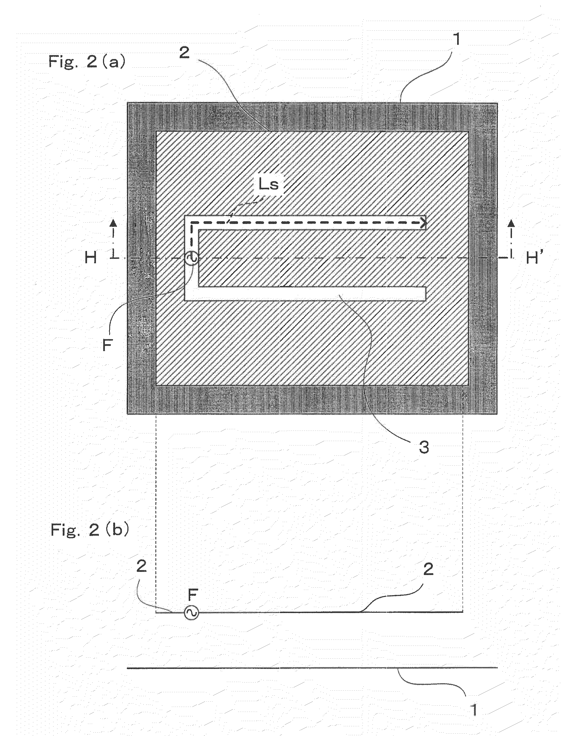
[0102]In the first embodiment (FIG. 1), the slot 3 of the conductor 2 has an arbitrary shape. However, when a slot 3A which has a well thought-out shape is used as illustrated in FIG. 12, the degree of coupling between the microstrip antenna, which is constituted of the ground conductor 1 and the conductor 2, and the slot 3A can be adjusted and the degree of freedom in design is enhanced as a result.
[0103]FIG. 12 is a plan view illustrating an RFID tag that constitutes a wireless communication device according to a second embodiment of the present invention, and uses the same reference symbols to denote the same components as those described above in order to omit detailed descriptions thereof.
[0104]FIG. 12 differs from the first embodiment in that a portion substantially parallel to the direction (broken-line arrow B) of the internal magnetic field of the microstrip antenna constituted of the ground conductor 1 and the conductor 2 is created by forming fold-back slot portions in tw...
third embodiment
[0120]In the first and second embodiments (FIG. 1 and FIG. 12), the capacitive coupling means 4a and 4b are formed from a structure stacked on top of the slot 3 of the conductor 2, but may instead be formed on the same plane as that of a slot 3B as illustrated in FIG. 15.
[0121]FIG. 15 is a plan view illustrating an RFID tag that constitutes a wireless communication device according to a third embodiment of the present invention, and uses the same reference symbols to denote the same components as those described above (see FIG. 1) in order to omit detailed descriptions thereof.
[0122]FIG. 15 differs from the first and second embodiments in that capacitive coupling means 4A and 4B are provided on a plane common to the slot 3B.
[0123]In this case, the capacitive coupling means 4A and 4B are each constituted of a third conductor, and the capacitive coupling means 4A is disposed adjacent to one side of the slot 3B whereas the capacitive coupling means 4B is disposed adjacent to the other ...
PUM
 Abstract
Description
Claims
Application Information
 - R&D
- Intellectual Property
- Life Sciences
- Materials
- Tech Scout
- Unparalleled Data Quality
- Higher Quality Content
- 60% Fewer Hallucinations
Browse by: Latest US Patents, China's latest patents, Technical Efficacy Thesaurus, Application Domain, Technology Topic, Popular Technical Reports.
© 2025 PatSnap. All rights reserved.Legal|Privacy policy|Modern Slavery Act Transparency Statement|Sitemap|About US| Contact US: help@patsnap.com