Chip carrier for a transponder module and transponder module

Active Publication Date: 2014-03-04
SMARTRAC INVESTMENT BV
View PDF22 Cites 0 Cited by
  • Summary
  • Abstract
  • Description
  • Claims
  • Application Information

AI Technical Summary

Benefits of technology

The present invention is aimed at providing a transponder module that can securely arrange the chip without causing significant thickening of the module's layer structure. The main goal is to protect the chip from mechanical stresses and minimize the impact on the module's performance.

Problems solved by technology

However, it is a drawback of this housing that it gives rise to the formation of a local thickening quickly emerging from the outer surface.
As a consequence, subsequent printing of the layer structure of the transponder module is rendered more difficult and the formation of an adhesive bonding connection which ensures uniform adhesion over the entire surface is impaired.

Method used


Image

  • Chip carrier for a transponder module and transponder module
  • Chip carrier for a transponder module and transponder module
  • Chip carrier for a transponder module and transponder module

Examples


Embodiment Construction

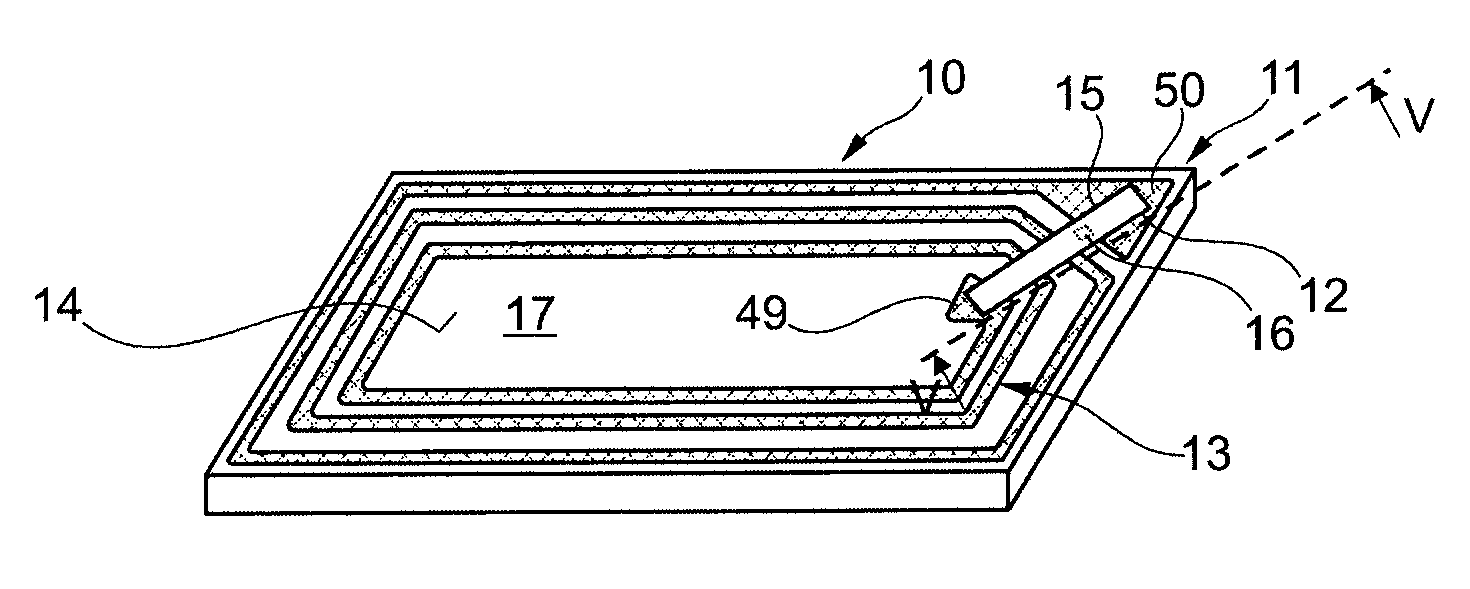
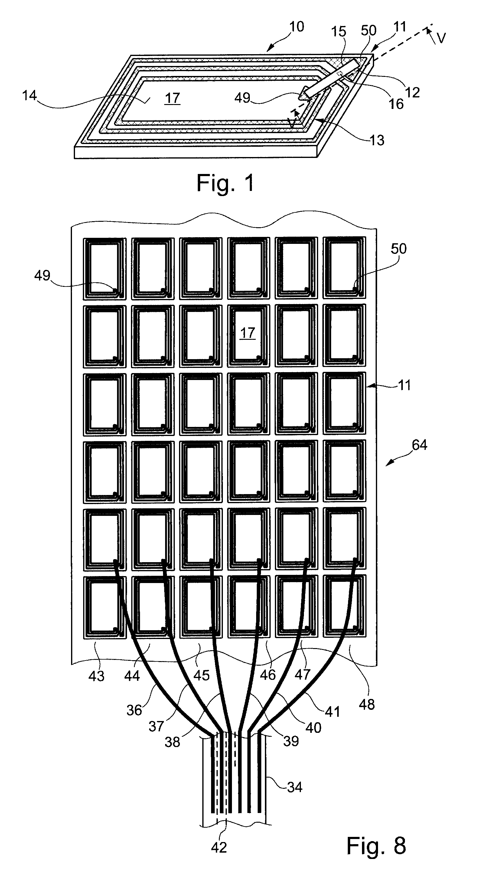
[0039]FIG. 1 shows a transponder module 10 comprising an antenna module 11 and a chip module 12. In the transponder module 10 shown in FIG. 1, the chip module 12 is located on the antenna side 14 of the antenna module which is equipped with an antenna 13, wherein a chip 16 disposed on a chip carrier 15 of the chip module 12 is received between the chip carrier 15 and an antenna substrate 17 of the antenna module 11.

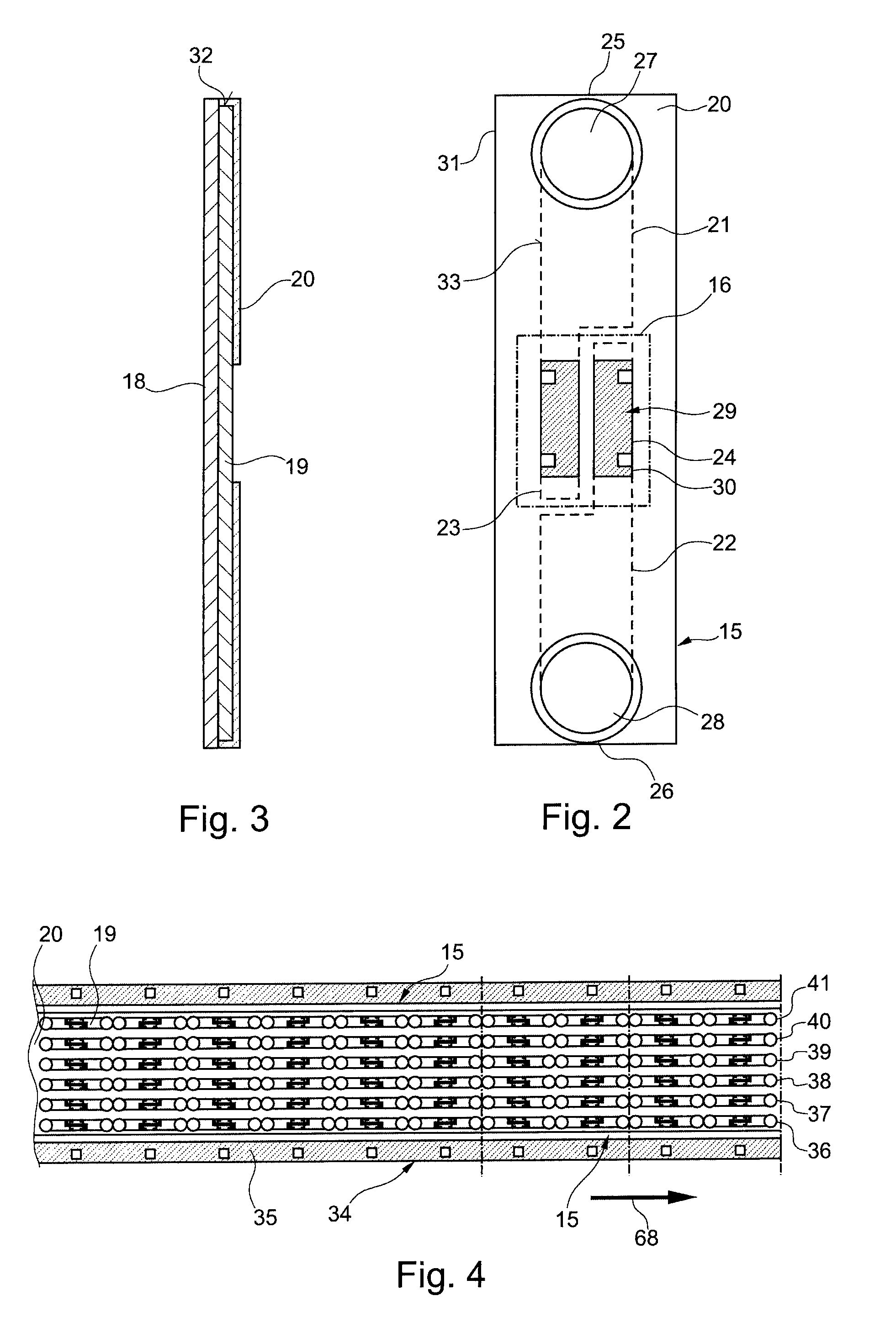
[0040]FIG. 2 shows the chip module 12 in a plan view, wherein for the purpose of better representation of the chip carrier 15, only the contours of the chip 16 are indicated.

[0041]As can be seen from a combined view of FIGS. 2 and 3, the chip carrier 15 is substantially configured as a three-layered structure comprising a carrier substrate 18 which, in the present case, is formed of PET, a contact metallization 19 applied to the carrier substrate 18 and here preferably composed of aluminum, and an insulation layer 20 which is disposed on the contact metallization 19.

[0042...


PUM


Abstract

A chip carrier for contacting with a chip and an antenna is disposed on an antenna substrate. The chip carrier features a carrier substrate having a chip contact arrangement located at a distance from longitudinal ends of the carrier substrate for electrical contacting with a chip. The carrier substrate includes two antenna contact surfaces having the chip contact arrangement therebetween for electrical contacting with the antenna. The chip contact arrangement and the antenna contact surfaces are located on an application surface of the chip carrier. At least one insulation surface-is formed on the application surface between the chip contact arrangement and the antenna contact surfaces.

Description

CROSS-REFERENCE TO RELATED APPLICATIONS[0001]This application claims priority to PCT International Application No. PCT / EP2009 / 002088 filed on Mar. 20, 2009, which claims the benefit of German Patent Application No. 10 2008 016 274.4 filed Mar. 28, 2008, both of which are incorporated herein by reference.STATEMENT REGARDING FEDERALLY SPONSORED RESEARCH OR DEVELOPMENT[0002]Not applicable.FIELD OF THE INVENTION[0003]The present invention relates to a chip carrier for contacting with a chip and an antenna disposed on an antenna substrate. Moreover, the present invention also relates to a chip carrier arrangement comprising a plurality of chip carriers which are disposed on a film-like sheet carrier. In addition, the present invention relates to a chip module comprising a chip carrier and a transponder module comprising a chip module disposed on an antenna module using a chip carrier. Finally, the present invention also relates to an antenna module for producing such a transponder module...

Claims


Application Information

Patent Timeline
IPC IPC(8): H01Q21/00
CPCG06K19/07779G06K19/07752H01L23/49855H01L2924/0002G06K19/07747G06K19/07783G06K19/07749H01L2924/00
Inventor RIETZLER, MANFREDFREEMAN, RAYMOND
Owner SMARTRAC INVESTMENT BV
Why Eureka
Try Eureka