Multilayer ceramic electronic component

a multi-layer ceramic and electronic component technology, applied in the direction of fixed capacitor details, stacked capacitors, fixed capacitors, etc., can solve the problems of difficult to form external electrodes with high precision, limited paste-applying precision in conventional thick-film paste firing methods, and deterioration of characteristics of multi-layer ceramic electronic components, so as to improve electrification efficiency, reduce the effect of plating time and efficient form of the plated film of the second external electrod

Active Publication Date: 2014-03-18
MURATA MFG CO LTD
View PDF20 Cites 8 Cited by
  • Summary
  • Abstract
  • Description
  • Claims
  • Application Information

AI Technical Summary

Benefits of technology

[0021]The dummy lead-through conductor is preferably disposed in the non-effective layer region so as to lead to at least two location of the superficies of the ceramic body, or, in other words, so as to lead through the ceramic body. In addition, the dummy lead-through conductor is preferably electrically connected to the second external electrode. Since the dummy lead-through conductor includes edges that are exposed at, at least, two locations of the superficies of the ceramic body, when a conductive medium, such as a steel ball, is brought into contact with one of the plurality of exposed edges of the dummy lead-through conductor, a current is also applied to the other exposed edges. This means that the probability of successful contact with the medium increases, which results in improved electrification efficiency. With this configuration, it is possible to reduce the plating time required to form a plated film as the underlying layer of the second external electrode.
[0022]Thus, even though the required size of a multilayer ceramic electronic component is decreasing, it is possible to efficiently form the plated film of the second external electrode efficiently.

Problems solved by technology

However, in general, the characteristics of a multilayer ceramic electronic component tend to deteriorate when the size of the multilayer ceramic electronic component is reduced because an effective area in which internal electrodes overlap one another is reduced.
Paste-applying precision in a conventional thick-film paste firing method is limited.
Therefore, it is difficult to form external electrodes with high precision when the conventional method is used.
However, even when the method disclosed in the Japanese Unexamined Patent Application Publication No. 2004-327983 is used, a problem of insufficient growth sometimes occurs when attempting to form a plated film by applying electrolytic plating to an electronic component having a small size of, for example, 1608 (approx.

Method used


Image

  • Multilayer ceramic electronic component
  • Multilayer ceramic electronic component
  • Multilayer ceramic electronic component

Examples


first preferred embodiment

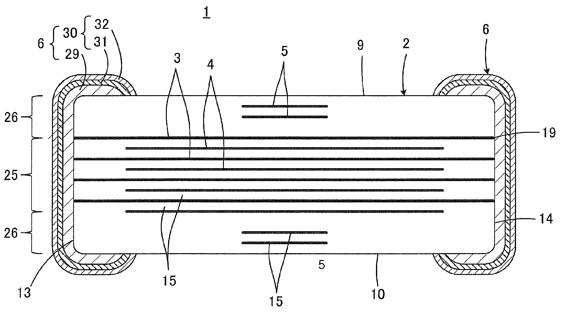
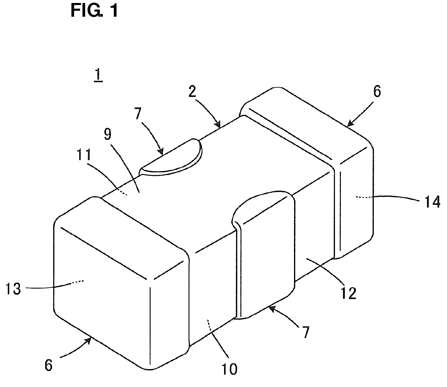
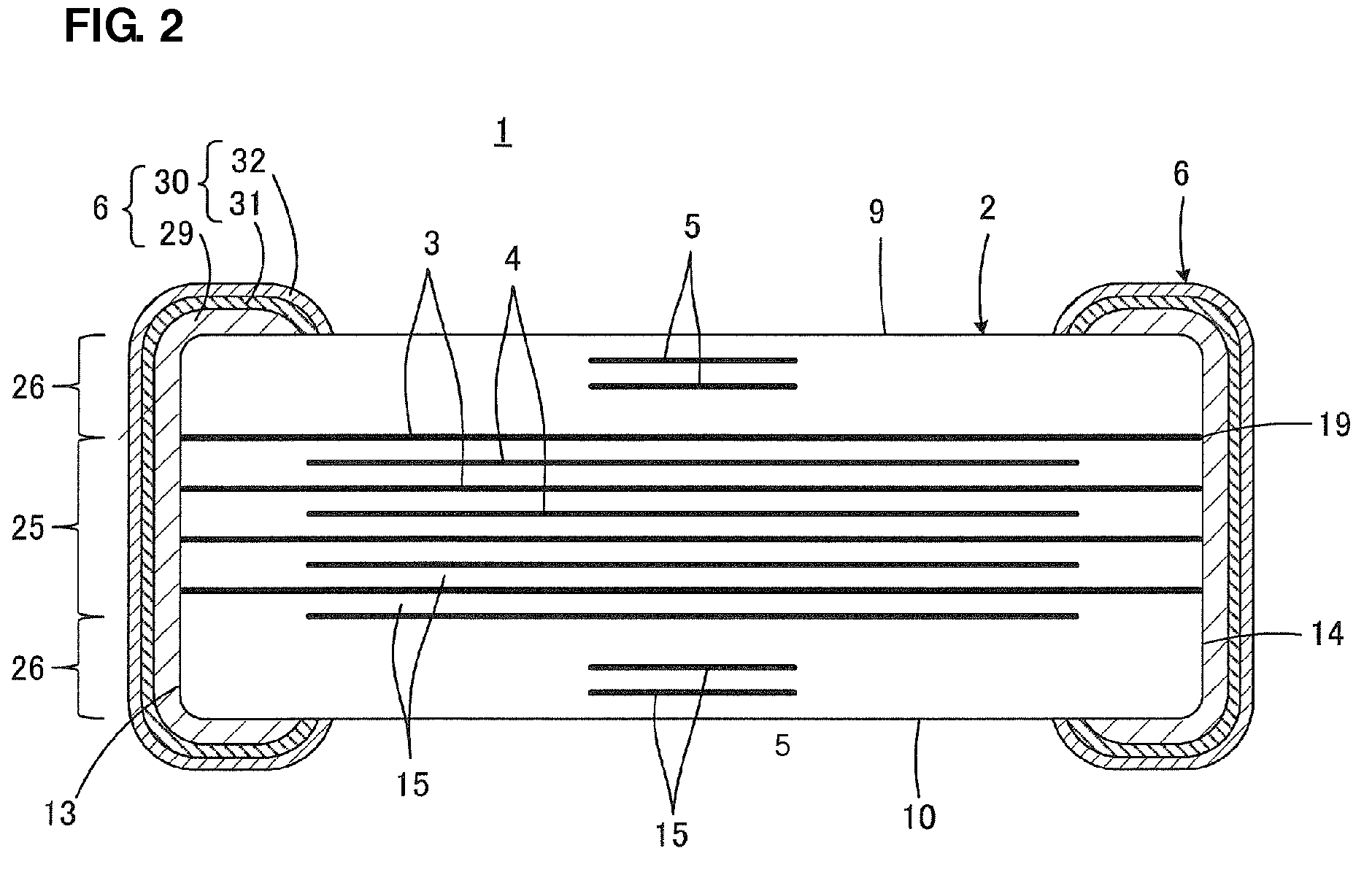
[0042]FIGS. 1 to 6 show a first preferred embodiment of the present invention. A multilayer ceramic capacitor 1 according to the first preferred embodiment of the present invention is a preferably three-terminal-type capacitor, for example. The multilayer ceramic capacitor 1 preferably includes a ceramic body 2, a first internal electrode group 3 and a second internal electrode group 4 that are provided inside the ceramic body 2, a dummy lead-through conductor 5 that is provided inside the ceramic body 2, and a first external electrode 6 and a second external electrode 7 that are provided on surfaces or superficies of the ceramic body 2. The structure of the multilayer ceramic capacitor 1 will be described in detail below.

[0043]The ceramic body 2 preferably has a substantially rectangular parallelepiped shape, for example. Specifically, the ceramic body 2 includes a first main surface 9 and a second main surface 10 that define a pair of opposite sides, a first side surface 11 and a ...

second preferred embodiment

[0083]A second preferred embodiment of the present invention is illustrated in FIGS. 7, 8, and 9. In FIGS. 7, 8, and 9, the same reference numerals are assigned to elements that correspond to those illustrated in FIGS. 1 to 6 to avoid redundant description.

[0084]A multilayer ceramic capacitor la according to the second preferred embodiment of the present invention preferably includes a second external electrode 7a including an underlying layer 33 and an upper layer 34 that is provided around the first side surface 11, the second side surface 12, the first main surface 9, and the second main surface 10 of the ceramic body 2.

[0085]In the process of growth that occurs during plating to form the underlying layer 33 of the second external electrode 7a, a plated film is preferably formed so as to surround the ceramic body 2. This increases the size of an electrode area that may function as a plating point for deposition. Therefore, electrification efficiency is improved, which increases t...

third preferred embodiment

[0092]A third preferred embodiment of the present invention is illustrated in FIGS. 10 to 14. In FIGS. 10 to 14, the same reference numerals are assigned to elements that correspond to those illustrated in FIGS. 1 to 6 to avoid redundant description.

[0093]A multilayer ceramic capacitor 1b according to the third preferred embodiment of the present invention preferably includes a first external electrode 6b in which an underlying layer 29b that is in contact with the exposed edge 19 of the first lead-out portion 18 of each of the plurality of first internal electrodes 3 is provided as a plated film.

[0094]Conditions for forming the plated film functioning as the underlying layer 29b described above are preferably the same or substantially the same as those for forming the plated film functioning as the underlying layer 33 of the second external electrode 7. Thus, it is possible to form the underlying layer 29b of the first external electrode 6b and the underlying layer of the second ex...


PUM

PropertyMeasurementUnit
thicknessaaaaaaaaaa
thicknessaaaaaaaaaa
thicknessaaaaaaaaaa

Abstract

In a multilayer ceramic electronic component, when a region of a ceramic body in layers where neither of a first internal electrode and a second internal electrode is provided as viewed in a direction in which a plurality of ceramic layers are stacked on one another is defined as a non-effective layer region, a dummy lead-through conductor is arranged in the non-effective layer region so as to lead to at least two locations on portions of superficies of the ceramic body and be electrically connected to a second external electrode. When a conductive medium is brought into contact with one of a plurality of exposed edges of the dummy lead-through conductor, a current is also applied to the other exposed edges.

Description

BACKGROUND OF THE INVENTION[0001]1. Field of the Invention[0002]The present invention relates to a multilayer ceramic electronic component. In particular, the present invention relates to a multilayer ceramic electronic component that includes external electrodes including plated films provided on the surfaces of a ceramic body.[0003]2. Description of the Related Art[0004]Electronic equipment such as mobile phones, notebook computers, digital cameras, and digital audio equipment is becoming more and more compact. A large number of multilayer ceramic electronic components that enable the size of such an electronic device to be reduced and the performance thereof to be improved are used therein.[0005]A typical multilayer ceramic electronic component includes a ceramic body that includes a plurality of ceramic layers formed on one another, internal electrodes formed inside the ceramic body, and an external electrode formed on a surface of the ceramic body. A multilayer ceramic electron...

Claims


Application Information

Patent Timeline
Patent Type & Authority Patents(United States)
IPC IPC(8): H01G4/005H01G4/06
CPCH01G4/30H01G4/232H01G4/012H01G4/005H01G4/12
Inventor AKAZAWA, TEPPEIHADANO, KENJIROSAKURATANI, MASAHIRO
Owner MURATA MFG CO LTD
Why Eureka
Try Eureka