
Integrated circuit test optimization using adaptive test pattern sampling algorithm

a technology of integrated circuit and sampling algorithm, which is applied in the direction of error detection/correction, instruments, computing, etc., can solve the problems of complex and expensive process of device testing in a manufacturing environment, wide range of faults of devices, and inevitable defects of semiconductor manufacturing

Inactive Publication Date: 2014-04-01
IBM CORP
View PDF18 Cites 5 Cited by
  • Summary
  • Abstract
  • Description
  • Claims
  • Application Information

AI Technical Summary

Benefits of technology

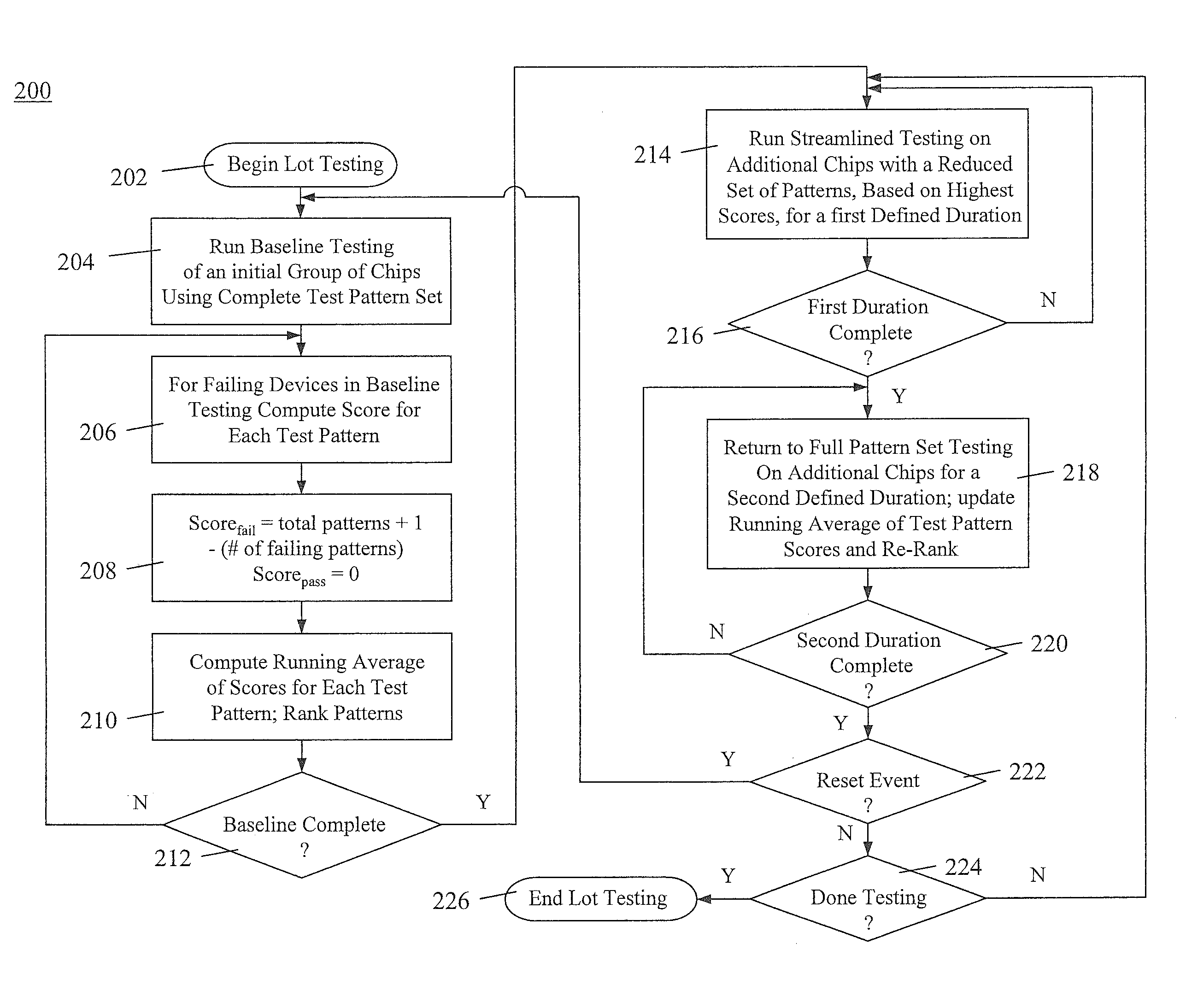
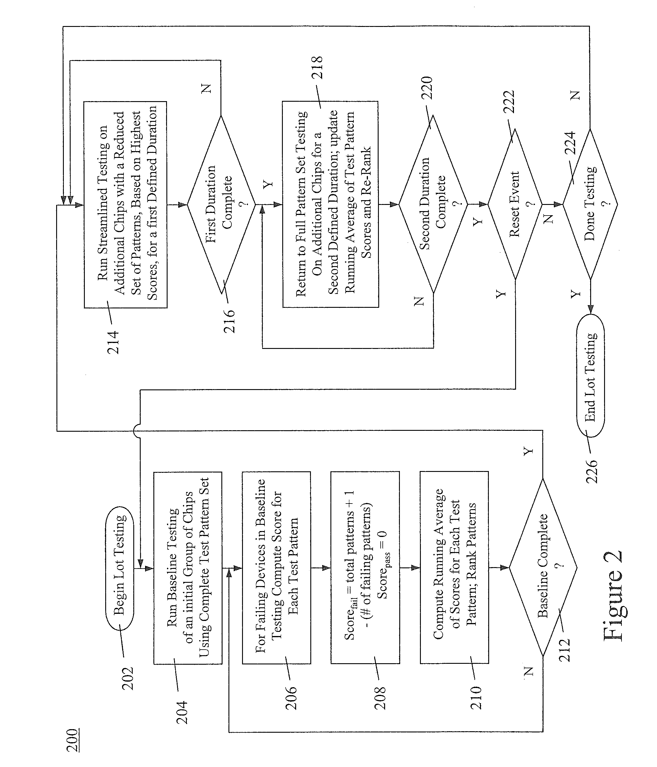
The patent describes a method and system for testing integrated circuit devices using adaptive test pattern selection. The method involves performing initial baseline testing of a group of chips, scoring each test pattern based on its ability to uniquely identify a failing chip. A reduced set of test patterns is then used for streamlined testing, followed by full testing using all available test patterns. During this process, the scoring of each test pattern is updated for each failing chip. The technical effect is that this method improves testing efficiency and accuracy.

Problems solved by technology

As with any other manufacturing process, defects inevitably arise during semiconductor manufacturing.
Device testing in a manufacturing environment can be a complex and expensive process.
Due to the increasing complexity of integrated circuit devices, the devices can suffer from a wide range of faults, such as shorts or opens in the semiconductor and wiring layers, stuck-at faults, and so on.
On the other hand, each test pattern that is run adds to the cost of the overall testing process of the devices.

Method used


Image

  • Integrated circuit test optimization using adaptive test pattern sampling algorithm
  • Integrated circuit test optimization using adaptive test pattern sampling algorithm
  • Integrated circuit test optimization using adaptive test pattern sampling algorithm

Examples


Embodiment Construction

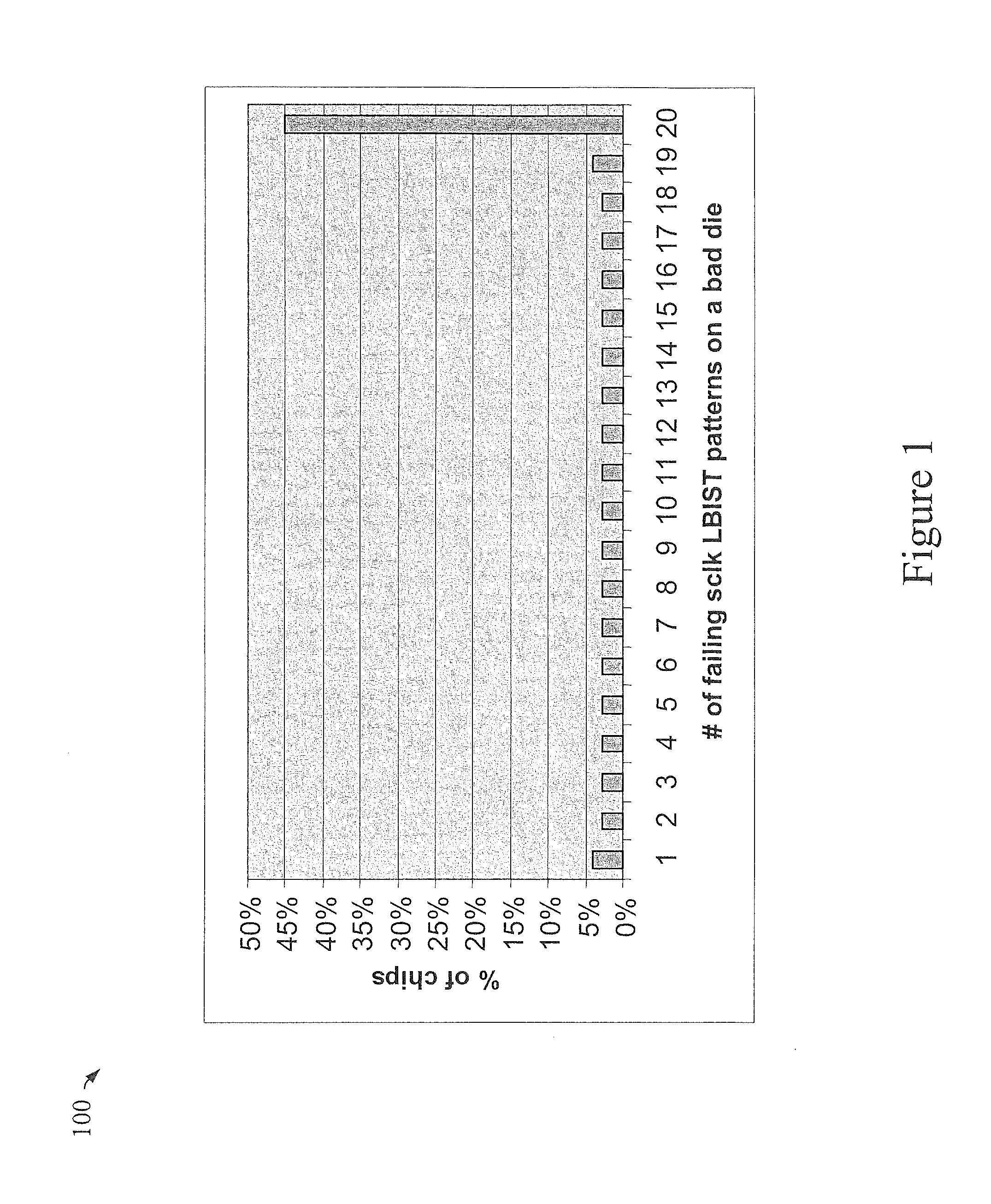
[0012]As indicated above, integrated circuit devices are subjected to large numbers (e.g., hundreds or even thousands) of test patterns in order to ensure defect detection. This is the case, even though it is generally recognized in the semiconductor industry that most defective devices can be caused to fail with many fewer tests than are typically run in a testing process. It is also well recognized that most of the time used to test digital integrated circuits is made up of the running of functional tests. However, the main problem in this regard is that it is not known ahead of time which ones of the available functional tests are going to catch a defective device. Therefore, IC manufacturers typically run all the tests available, and therefore much test time is wasted. Efforts may be made to look at historical pass / fail information with respect to functional test fails, followed by reducing the pattern list, but such a process is iterative and backward looking.

[0013]Pattern rank...


PUM


Abstract

A method of implementing integrated circuit device testing includes performing baseline testing of a first group of chips using a full set of test patterns, and for chip identified as failing, determining, a score for each test pattern in the full set. The score is indicative of an ability of the test pattern to uniquely identify a failing chip with respect to other test patterns. Following the baseline testing, streamlined testing on a second group of chips is performed, using a reduced set of the test patterns having highest average scores as determined by the baseline testing. Following the streamlined testing, full testing on a third group of chips is performed using the full set of test patterns, and updating the average score for each pattern. Further testing alternates between the streamlined testing and the full testing for additional groups of chips.

Description

BACKGROUND[0001]The present invention relates generally to semiconductor device manufacturing and, more particularly, to integrated circuit test optimization using an adaptive test pattern sampling algorithm.[0002]Semiconductor devices are typically fabricated in large lots on semiconductor wafers. The fabrication process includes various steps such as, for example, deposition, lithography, etching, sputtering, and other techniques known to those skilled in the art. As with any other manufacturing process, defects inevitably arise during semiconductor manufacturing. These defects must be detected by the manufacturer before completed integrated circuit devices are delivered to customers.[0003]Device testing in a manufacturing environment can be a complex and expensive process. Due to the increasing complexity of integrated circuit devices, the devices can suffer from a wide range of faults, such as shorts or opens in the semiconductor and wiring layers, stuck-at faults, and so on. To...

Claims


Application Information

Patent Timeline
IPC IPC(8): G01R31/28
CPCG06F11/263G01R31/31835
Inventor GRADY, MATTHEW S.JOHNSON, MARK C.PEPPER, BRADLEY D.PERCY, DEAN G.PRANYS, JOSEPH C.
Owner IBM CORP
Learn More