
Contact probe device having a substrate fitted into slits of cylindrical electrodes

a cylindrical electrode and contact probe technology, applied in the direction of coupling contact members, instruments, printed circuits, etc., can solve the problems of requiring thousands of man-hours for building a test model, solder balls can be hardly used as terminals, solder balls deformed, etc., to achieve stable contact, easy and surely satisfactory frequency characteristics, the effect of ensuring the accuracy

Inactive Publication Date: 2014-04-08
ELMEC
View PDF13 Cites 2 Cited by
  • Summary
  • Abstract
  • Description
  • Claims
  • Application Information

AI Technical Summary

Benefits of technology

The contact probe device of this patent allows for independent elastic contact between individual cylindrical electrodes and external electrodes, making sure stable contact is easily and securely realized in both chip-like electronic components and ultra high frequency ranges. The flexible insulating substrate allows for further stable contact even if the chip-like electronic component is deformed. The device also provides a space for storing the electronic component, facilitating positioning. A metal guide plate is provided for easy fixation to the mounting substrate and a pressing member is supported by the metal guide plate for further secure contact. The pressing member has a nut member and screw member for detachable and attachable pressing of the electronic component to the cylindrical electrodes.

Problems solved by technology

However, in the electronic component having the ball grid array (BGA) structure, in an experimental stage, when the electronic component is soldered to connect to the mounting substrate by manual work using a soldering iron, the solder balls are deformed at the moment when the iron is brought into contact with the solder balls, and there is a tendency that such solder balls can be hardly used as terminals.
Then, the electronic component is hardly connected to the mounting substrate with hand solder, thus requiring thousands of man-hours for building a test model.
However, in the electronic component with the chip structure, when there is a large number of terminals, there is a problem that when the electronic component needs to be desoldered in a case of re-adjustment or change of a constant after being soldered to the mounting substrate, the electronic component is hardly desoldered, thus damaging the mounting substrate in some cases.

Method used


Image

  • Contact probe device having a substrate fitted into slits of cylindrical electrodes
  • Contact probe device having a substrate fitted into slits of cylindrical electrodes
  • Contact probe device having a substrate fitted into slits of cylindrical electrodes

Examples


Embodiment Construction

[0029]Preferred embodiments of the present invention will be described hereafter, with reference to the drawings.

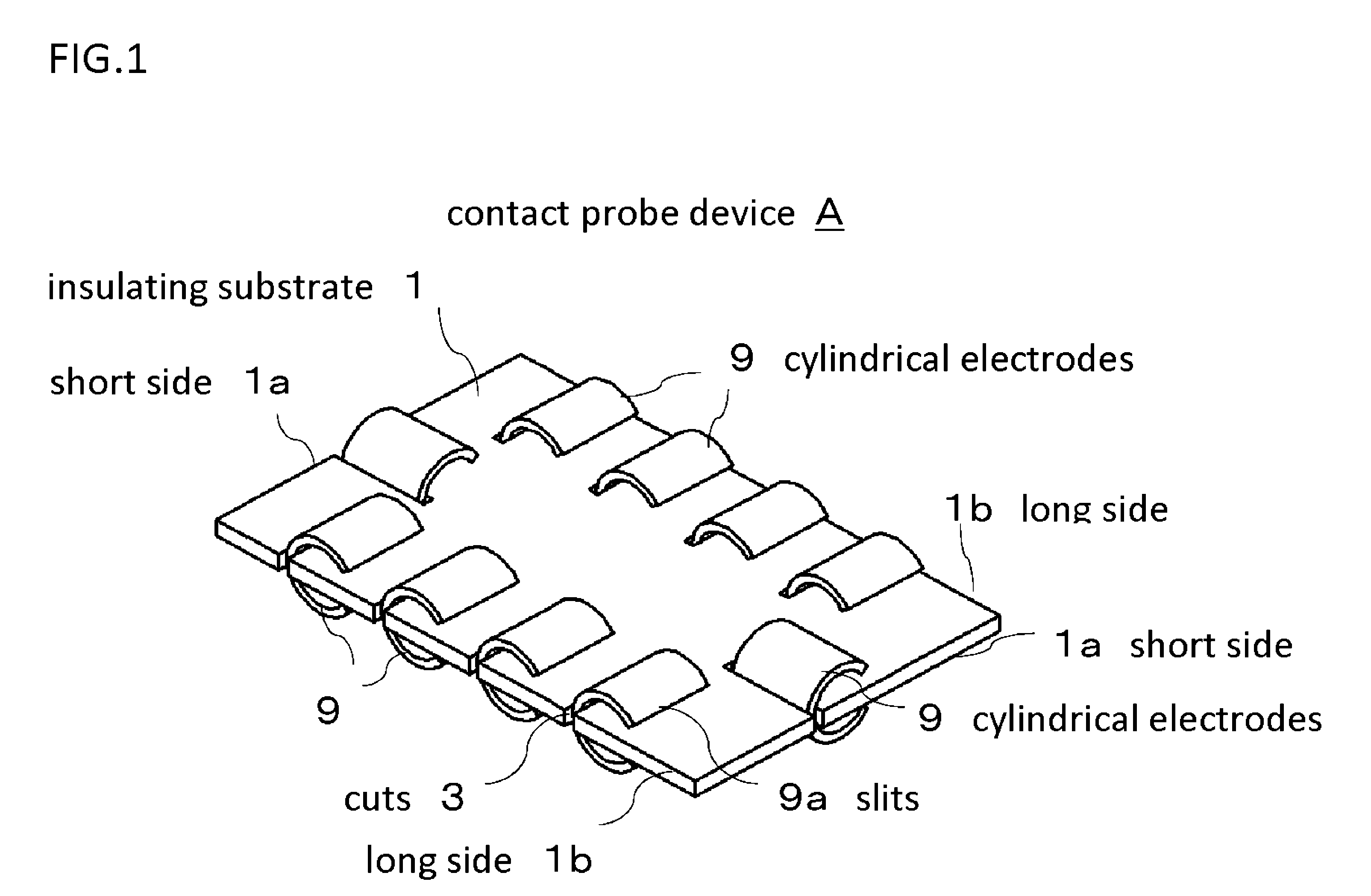
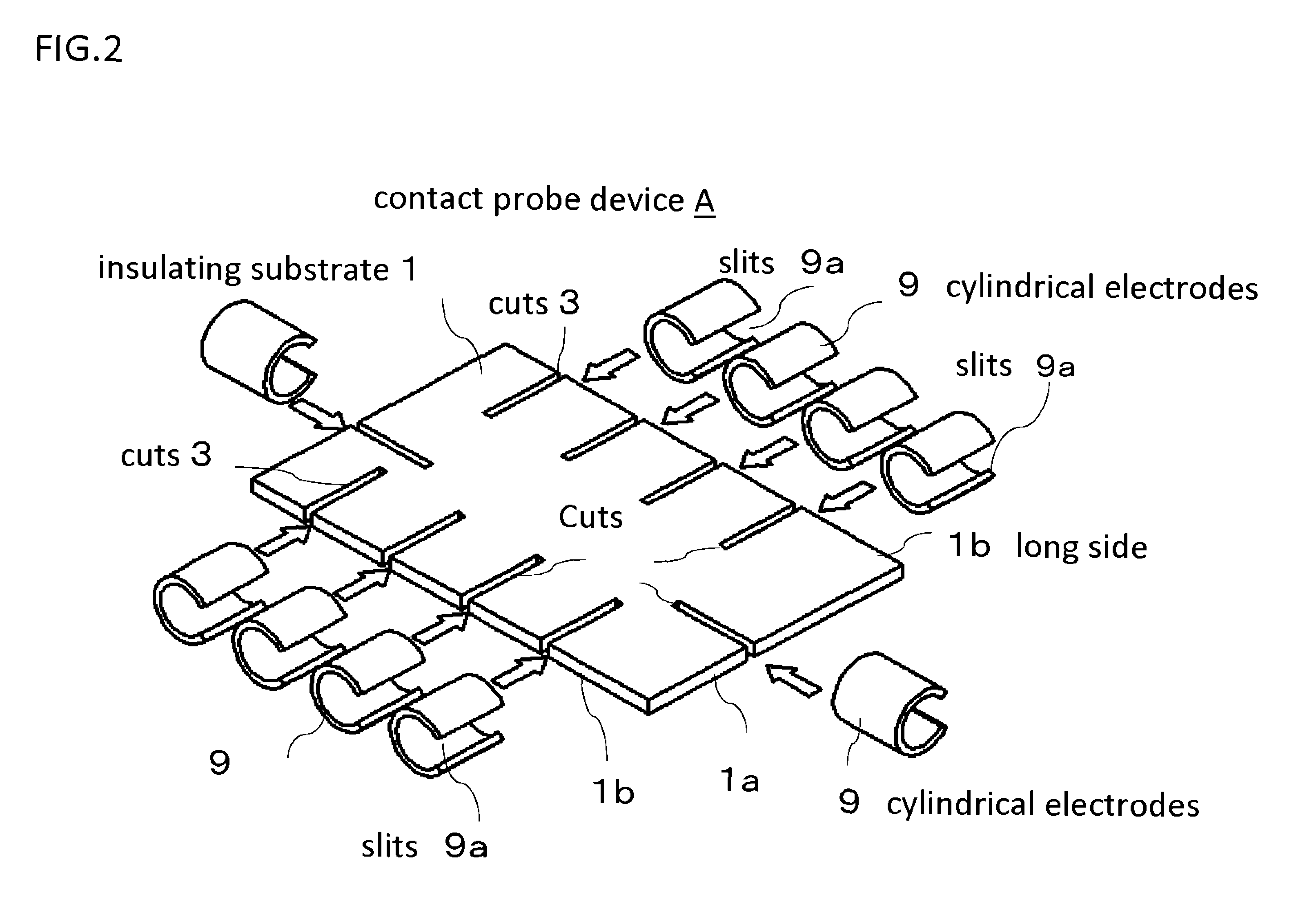
[0030]FIG. 1 and FIG. 2 are a perspective view and an exploded perspective view of a contact probe device A according to an embodiment of the present invention.

[0031]In FIG. 1 and FIG. 2, insulating substrate 1 has flexibility and is a thin substrate with a thickness of 0.2 mm, which is made of a publicly-known excellent insulating resin material having flexibility and satisfactory frequency loss characteristics, and which is formed into, for example, a rectangular shape with a long side of 6 mm and a short side of 4 mm, and a plurality of cuts 3 cut by 1.2 mm from the outer peripheral end, such as one on the opposed short sides 1a respectively, and four on the opposed long sides 1b respectively.

[0032]The cuts 3 are formed at formation pitches (intervals) of the electrodes 7 for external connection provided on the outer periphery of an electronic component 5 as will be de...


PUM


Abstract

To obtain a satisfactory contact state in an ultra high frequency range with a low loss, in a contact probe device with an electronic component connected to a mounting substrate. Insulating substrate 1 has cuts 3 with narrow width formed from an outer peripheral end. Cylindrical electrodes 9 are made of a conductive material and have slits 9a extending in its axial direction. A plurality of cylindrical electrodes 9 are supported by the insulating substrate 1 in such a manner as being inserted into each cuts 3 so that the insulating substrate 1 is fitted into each slit 9a.

Description

TECHNICAL FIELD[0001]The present invention relates to a contact probe device, and relates to an improvement of the contact probe device for connecting a component such as a chip-like electronic component to a mounting substrate in an electronic device.DESCRIPTION OF RELATED ART[0002]In recent years, an electronic component mounted on a mounting substrate, which can be used in an ultra high speed frequency range exceeding 10 GHz, has been requested, in accordance with an increase in a speed of an operation in an electronic circuit formed on the mounting substrate in an electronic device.[0003]In order to prevent deterioration of the frequency characteristics due to inductance components of terminals formed in an electronic component, the electronic component that can be used in the ultra high speed frequency range has generally a leadless chip structure or a ball grid array (BGA) structure constituted of solder balls.[0004]However, in the electronic component having the ball grid arr...

Claims


Application Information

Patent Timeline
Patent Type & Authority Patents(United States)
IPC IPC(8): H01R12/00
CPCH01R12/718H01R13/24
Inventor SHIGA, MOTOTSUGU
Owner ELMEC
Learn More