Semiconductor embedded module and method for producing the same

a technology of embedded modules and semiconductors, applied in the direction of semiconductor devices, solid-state devices, basic electric elements, etc., can solve the problems of difficult high-precision alignment between an external connection pad of an ic chip and a via, circuit damage of the ic chip or the distribution layer of the csp, etc., and achieve the effect of producing the embedded modul

Active Publication Date: 2014-06-03
TDK CORPARATION
View PDF20 Cites 17 Cited by
  • Summary
  • Abstract
  • Description
  • Claims
  • Application Information

AI Technical Summary

Benefits of technology

[0008]The present invention has been made in light of the above circumstances, and therefore has an object to provide a semiconductor embedded module which, when forming a via for external connection for a semiconductor device, can prevent a circuit or wiring of the semiconductor device from being damaged, and to provide a method for producing the same.
[0010]In the semiconductor embedded module with the above structure, when grinding the second insulating layer in order to form a via on the external connection pad for external connection of the semiconductor device, even if the via formation position is dislocated from the target position, the semiconductor device is protected by the first insulating layer because the grinding rate of the second insulating layer is larger than that of the fist insulating layer; in other words, the first insulating layer is more difficult to be ground than the second insulating layer. Accordingly, the circuit and internal wiring of the semiconductor device are not damaged due to grinding.
[0011]As described above, even if the via opening position is slightly dislocated from the position of the external connection pad, in other words, the via is opened on at least a part of the external connection pad and at least a part of the first insulating layer, wiring can be reliably drawn to the outside without damaging the semiconductor device.
[0013]Further, the method for producing a semiconductor embedded module according to the invention is a method for effectively producing the semiconductor embedded module of the invention, and the method includes the steps of: preparing a semiconductor device which is provided with a wiring layer; providing a first insulating layer in the periphery of the wiring layer such that an external connection pad of the wiring layer is exposed; providing, on the first insulating layer, a second insulating layer having a grinding rate larger than that of the first insulating layer; and grinding a part of the second insulating layer which is on the external connection pad to form a via to have the external connection pad exposed. Here, the step of providing a mask which is provided with an opening corresponding to a portion of the second insulating layer which is above the external connection pad may further be implemented, and in the step of having the external connection pad exposed, the second insulating layer may be ground through blasting treatment to form a via.
[0014]Moreover, employing wet blasting for blasting treatment is useful because, in comparison with dry blasting, wet blasting easily prevents electrification.
[0015]According to the invention, since the grinding rate of the second insulating layer provided on the first insulating layer provided in the periphery of the semiconductor device is larger than the grinding rate of the first insulating layer, when grinding the second insulating layer in order to form the via on the external connection pad for the semiconductor device, even if the via formation position is dislocated from the target position, the semiconductor device is protected by the first insulating layer. Accordingly, the circuit and internal wiring of the semiconductor device can be reliably prevented from being damaged due to grinding.

Problems solved by technology

However, as described above, with downsizing and a reduction in pitch of a device or component, alignment between an external connection pad of the IC chip and a via has been becoming difficult to be performed with high precision.
If the via is opened at the position where the via is dislocated from the external connection pad of the IC chip, the circuit of the IC chip or distribution layer of the CSP may be damaged when the circuit or redistribution layer is at the opening position.

Method used


Image

  • Semiconductor embedded module and method for producing the same
  • Semiconductor embedded module and method for producing the same
  • Semiconductor embedded module and method for producing the same

Examples


Embodiment Construction

[0021]An embodiment of the invention will hereinafter be described in detail. Note that like components are denoted by like reference symbols and will not be further explained. It is assumed that vertical and horizontal positional relations are based on the positional relations shown in the drawings, unless otherwise specified. Also, the dimensional ratios of the drawings are not limited to a shown ratio. Moreover, the following embodiment is for explaining the invention, and is not intended to limit the invention to the embodiment only. Furthermore, various modifications of the invention may be made without departing from the gist of the invention.

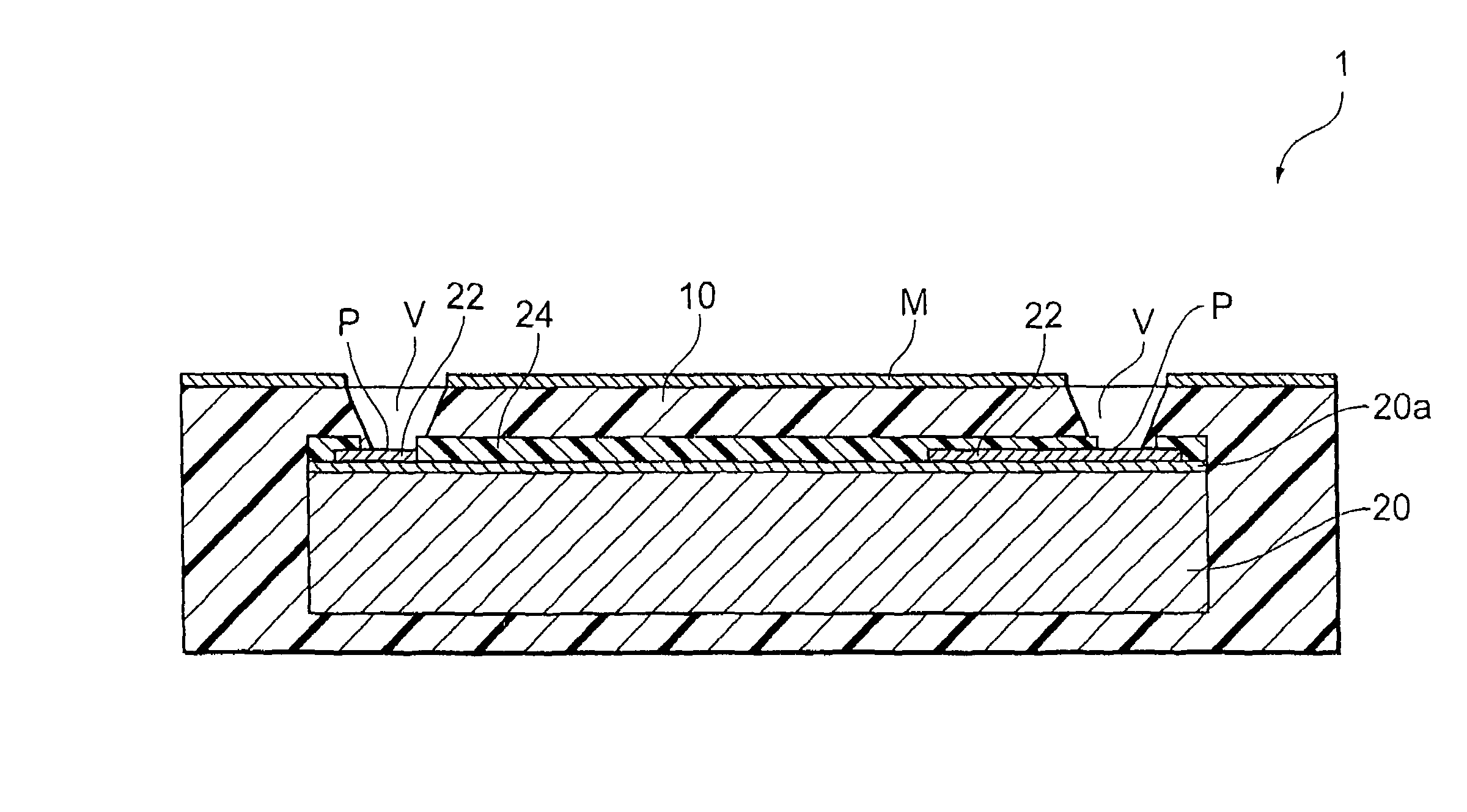
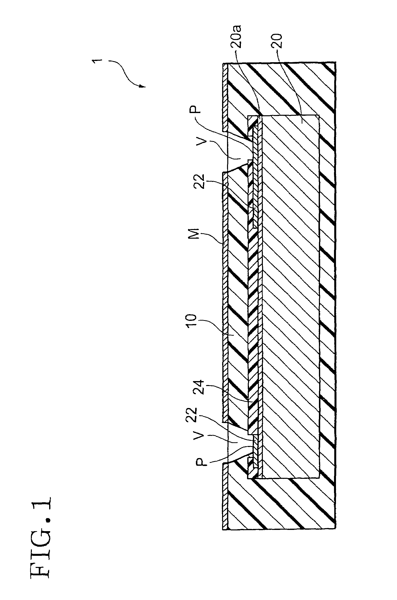
[0022]FIG. 1 is a sectional view showing a schematic configuration of an embodiment of a semiconductor embedded module according to the invention. A semiconductor embedded module 1 has a configuration in which a semiconductor device 20, which is an electronic component such as a semiconductor IC (die) in a bare chip state, is embedded in ...


PUM

PropertyMeasurementUnit
insulatingaaaaaaaaaa
densityaaaaaaaaaa
thicknessaaaaaaaaaa

Abstract

A semiconductor embedded module 1 of the present invention has a configuration in which a semiconductor device 20, which is an electronic component such as a semiconductor IC (die) in a bare chip state, is embedded in a resin layer 10 (second insulating layer). In the semiconductor device 20, a redistribution layer 22 is connected to land electrodes. A protective layer 24 (first insulating layer) is provided on the redistribution layer 22, and is provided with openings such that external connection pads P of the redistribution layer 22 are exposed. Also, the resin layer 10 is formed to cover the protective layer 24, and vias V are formed at the positions of the respective external connection pads P of the redistribution layer 22. The grinding rate of the resin layer 10 is larger than that of the protective layer 24.

Description

CROSS-REFERENCES TO RELATED APPLICATIONS[0001]The present application is based on Japanese priority application No. 2008-186864, filed on Jul. 18, 2008, the entire contents of which are hereby incorporated by reference.BACKGROUND[0002]1. Technical Field[0003]The present invention relates to a semiconductor embedded module and a method for producing the same.[0004]2. Related Art[0005]Generally, a substrate which is provided with an electronic component (electronic component-embedded substrate) such as a semiconductor device (an IC chip or other type of semiconductor active element) has a structure in which a semiconductor device (die) in a bare chip state is fixed to a substrate constituted by a single resin layer or plural resin layers. In order to respond to the demand for higher performance and downsizing of electronic equipment, modules are now being provided with higher-density packaging of active components such as semiconductor devices and passive components such as resistors ...

Claims


Application Information

Patent Timeline
Patent Type & Authority Patents(United States)
IPC IPC(8): H01L23/48
CPCH01L2924/14H01L2924/0103H01L2924/01015H01L2924/01006H01L2924/01019H01L23/3107H01L23/3114H01L2924/01012H01L2924/0102H01L2924/01013H01L2924/01029H01L23/3171H01L2924/01057H01L24/82H01L2924/01082H01L2924/19043H01L2924/01038H01L2924/0104H01L2924/01023H01L24/18H01L2924/19041H01L2924/01033H01L2924/04953H01L2224/04105H01L2924/01073H01L2924/01003H01L2224/82047H01L2224/18H01L24/24H01L2224/023H01L2224/96H01L2924/1815H01L2924/0001
Inventor KAWABATA, KENICHIENDO, TOSHIKAZU
Owner TDK CORPARATION
Why Eureka
Try Eureka