Microchip with blocking apparatus and method of fabricating microchip

a technology of blocking apparatus and microchip, which is applied in the field of microchips, can solve the problems of compromising the integrity and performance of the ultimately produced microchip, short circuit, and significant yield loss

Active Publication Date: 2014-06-10
ANALOG DEVICES INC
View PDF12 Cites 2 Cited by
  • Summary
  • Abstract
  • Description
  • Claims
  • Application Information

AI Technical Summary

Benefits of technology

[0004]The inventors discovered that metal bonds in their liquid form (i.e., during the bonding step of fabrication) often oozes onto the underlying die, consequently compromising the integrity and performance of the ultimately produced microchip. For example, the inventors noticed that this liquid metal can contact the interconnect pads, causing a short circuit. This often produces significant yield loss, thus increasing microchip fabrication costs.
[0005]In accordance with one embodiment of the invention, a method of forming a microchip provides a base die and a cap die. The base die has a top surface with an exposed conductive interconnect, and an isolation trench around the conductive interconnect. The method also adds metal to one or both the cap die and the base die, and places the cap die and base die together to form an intermediate apparatus having a blocking apparatus. The intermediate apparatus forms an uncured metal seal from the added metal on the one or both dies. The blocking apparatus is positioned between the uncured metal seal and the interconnect. Metal from the uncured metal seal migrates toward the conductive interconnect. The blocking apparatus thus contacts the migrating metal to prevent such metal from contacting the interconnect—and preferably from electrically connecting the interconnect and the metal seal. Finally, the method allows the metal seal to cool, forming a metal seal.
[0010]In accordance with another embodiment, a microchip has a base die with a conductive interconnect and an isolation trench around at least a portion of the conductive interconnect, and a cap die secured to the base die. A seal, formed from a metal material, is positioned between the base die and the cap die to secure them together. The microchip also has a protrusion, which extends downwardly from the cap die. The protrusion is spaced from, and does not contact, the base die. The protrusion at least in part prevents the metal material from contacting both the interconnect and the seal.

Problems solved by technology

The inventors discovered that metal bonds in their liquid form (i.e., during the bonding step of fabrication) often oozes onto the underlying die, consequently compromising the integrity and performance of the ultimately produced microchip.
For example, the inventors noticed that this liquid metal can contact the interconnect pads, causing a short circuit.
This often produces significant yield loss, thus increasing microchip fabrication costs.
The metal in this embodiment may have leaked from the seal and into the trench.

Method used


Image

  • Microchip with blocking apparatus and method of fabricating microchip
  • Microchip with blocking apparatus and method of fabricating microchip
  • Microchip with blocking apparatus and method of fabricating microchip

Examples


Embodiment Construction

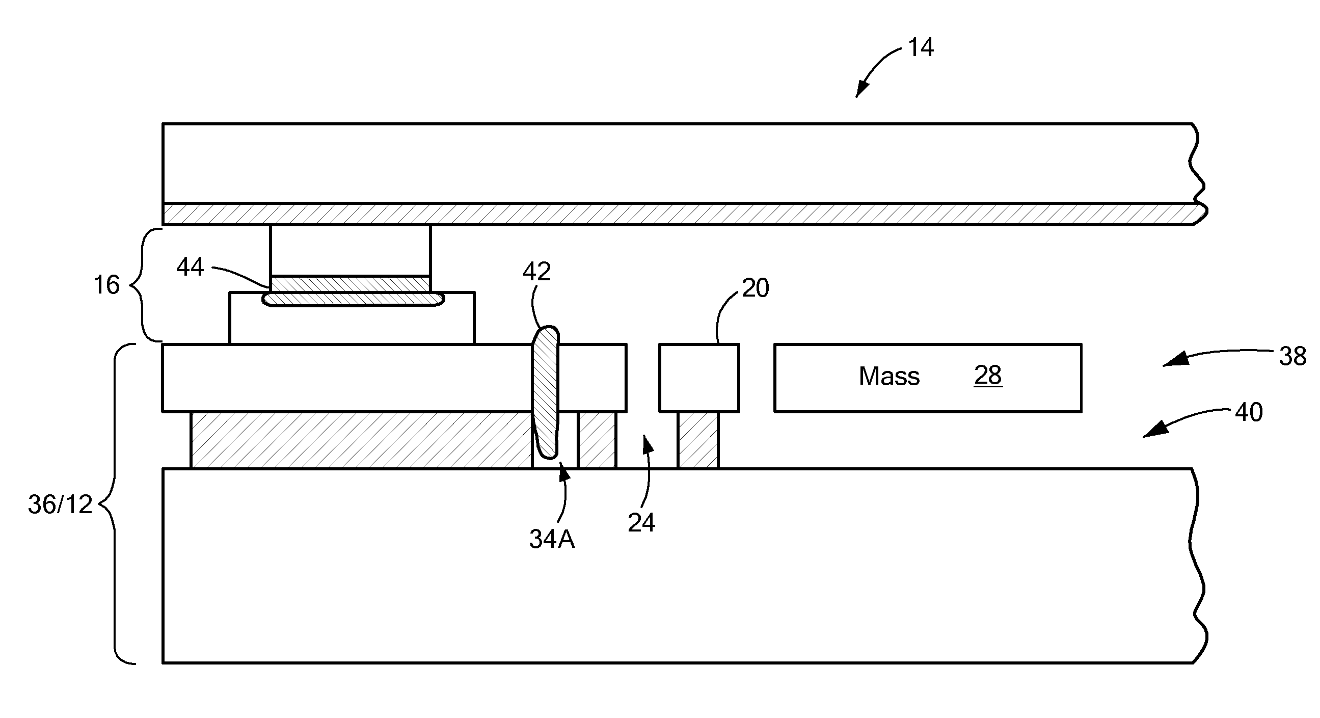
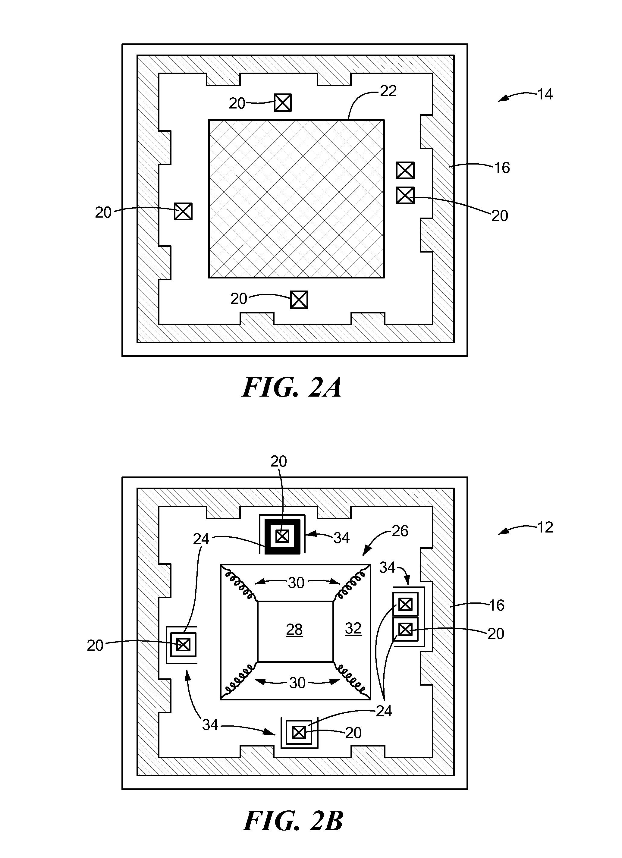
[0022]In illustrative embodiments, a microchip is configured to minimize yield loss during fabrication. To that end, the microchip has a blocking apparatus that, during fabrication, prevents liquid metal from electrically connecting its electrical interconnect (e.g., a bond pad) with a metal seal coupling its cap and base dies. For example, among other things, the blocking apparatus may include a blocking trench in the base wafer to capture overflowing liquid metal during the fabrication process. As a second example, the blocking apparatus also may include a protrusion, extending downwardly from the cap wafer, that uses surface tension to retain the liquid metal. Details of illustrative embodiments are discussed below.

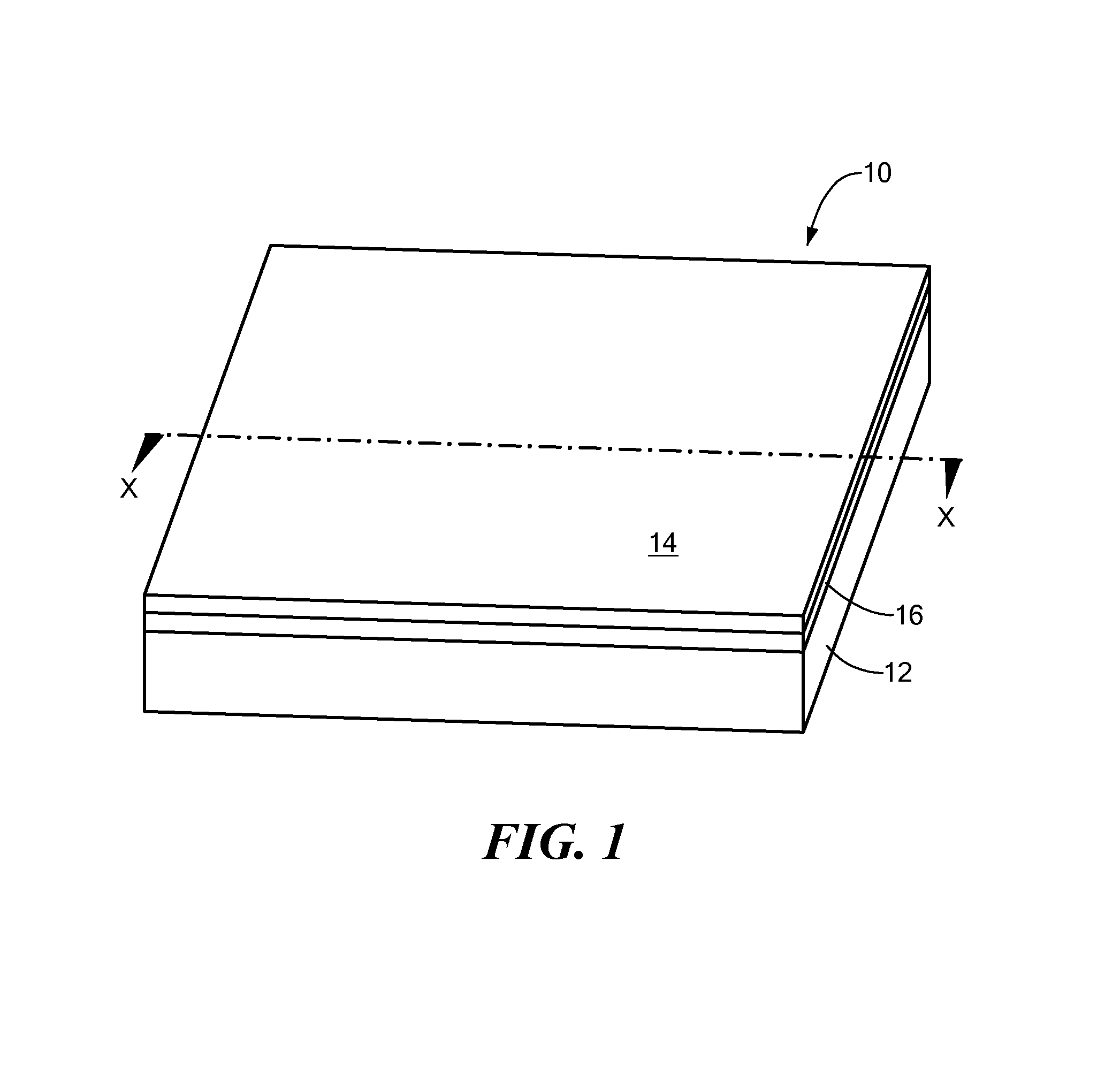
[0023]FIG. 1 schematically shows a microchip 10 that may be configured in accordance with illustrative embodiments of the invention. Specifically, the microchip 10 may be considered to be a wafer level chip scale package (“WLCSP”) formed from two dies 12 and 14 bonded ...


PUM


Abstract

A microchip has a base die with a conductive interconnect and an isolation trench around at least a portion of the conductive interconnect, and a cap die secured to the base die. A seal, formed from a metal material, is positioned between the base die and the cap die to secure them together. The microchip also has a blocking apparatus, between the isolation trench and the metal seal, that at least in part prevents the metal material from contacting the interconnect.

Description

FIELD OF THE INVENTION[0001]The invention generally relates to microchips and, more particularly, the invention relates to bonding microchips together.BACKGROUND OF THE INVENTION[0002]A wide variety of microchips use caps to protect their interior components. For example, micro-electromechanical systems (“MEMS devices”) often have a cap to protect their fragile microstructure. Many MEMS devices typically have a glass seal to bond the silicon die caps to the underlying MEMS chip. Such a seal, which can be hermetic, may have widths on the order of about 150 to 400 microns. Undesirably, this seal footprint increases die size. As a consequence, fewer dies / microchips can be formed from individual wafers, thus increasing per-unit fabrication costs.[0003]The art has responded to this problem by using metal to bond the cap dies / wafers to the underlying device dies / wafers. Specifically, metal can provide bonds and hermeticity comparable to seal glass, but with smaller widths. Accordingly, me...

Claims


Application Information

Patent Timeline
Patent Type & Authority Patents(United States)
IPC IPC(8): H01L23/06H01L23/34H01L23/02
CPCB81C2203/019B81B7/007B81C2203/035B81C3/001B81C1/00269B81C2203/0109
Inventor CHEN, LINUNAN, THOMAS KIERANYANG, KUANG L.
Owner ANALOG DEVICES INC
Why Eureka
Try Eureka