
Clock distribution using MTJ sensing

a clock distribution and mtj technology, applied in the direction of generating/distributing signals, pulse techniques, instruments, etc., can solve the problems of increasing routing overhead, inability to maintain the uniformity of branches in an h-tree structure b>100/b>, and significant power consumption of clock distribution networks

Inactive Publication Date: 2014-07-15
QUALCOMM INC
View PDF10 Cites 1 Cited by
  • Summary
  • Abstract
  • Description
  • Claims
  • Application Information

AI Technical Summary

Benefits of technology

The present patent text describes an apparatus for distributing clock signals using magnetic tunnel junctions (MTJs) on a chip. The apparatus includes a first clocked circuit and clock generation circuitry with a magnetic field sensing device and amplifier circuitry. The clock generation circuitry senses an oscillating magnetic field and converts it into a clock signal. The technical effect of this invention is that it provides a reliable and efficient mechanism for distributing clock signals to different parts of the chip, which can improve the synchronization and performance of the chip.

Problems solved by technology

A significant amount of power is consumed by clock distribution networks that provide clock signals to numerous clocked circuits of systems on chip (SOC).
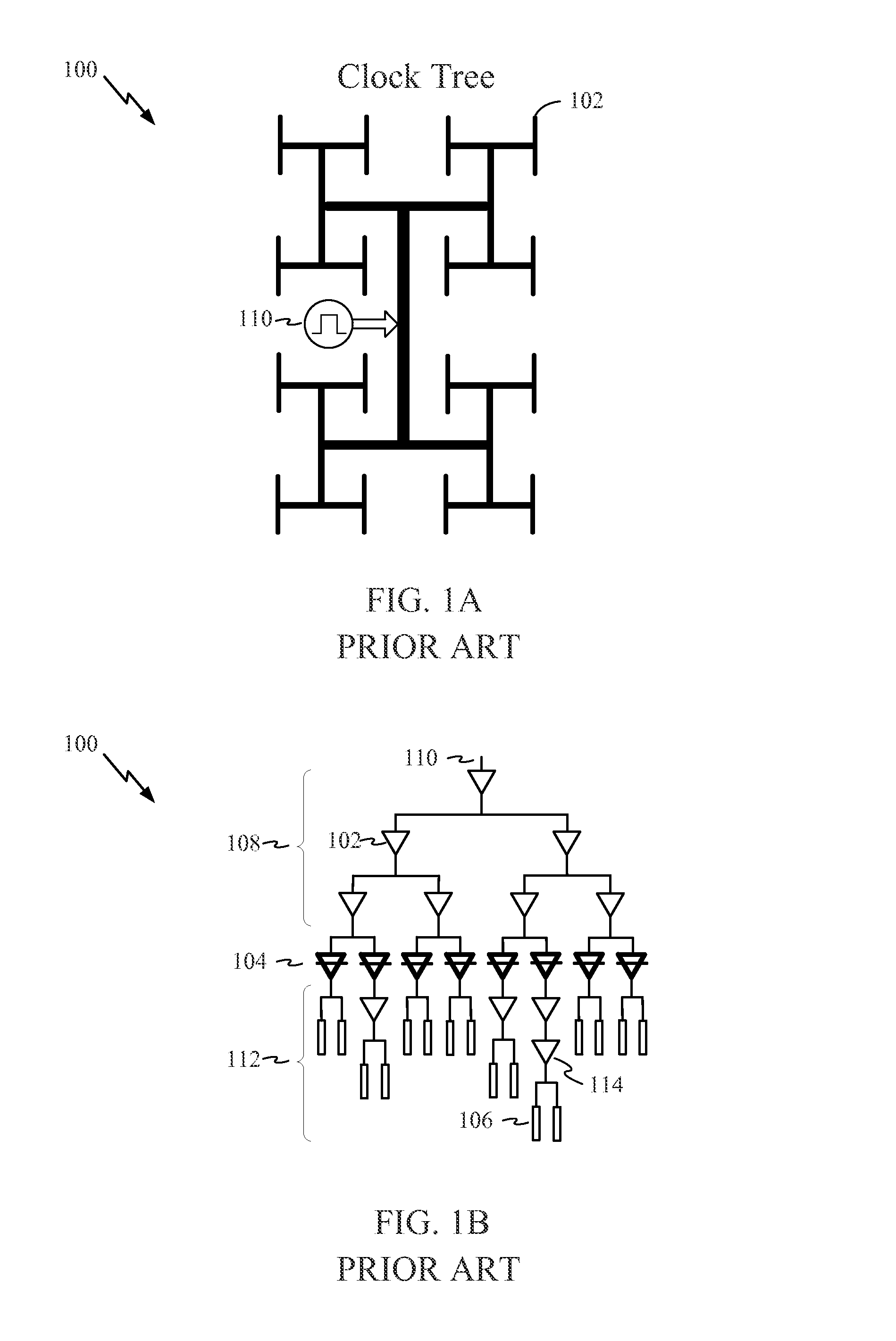
However, the uniformity of branches in an H-tree structure 100 cannot be maintained across increasingly complex devices, which may include millions of clocked circuits, such as logic gates, for example.
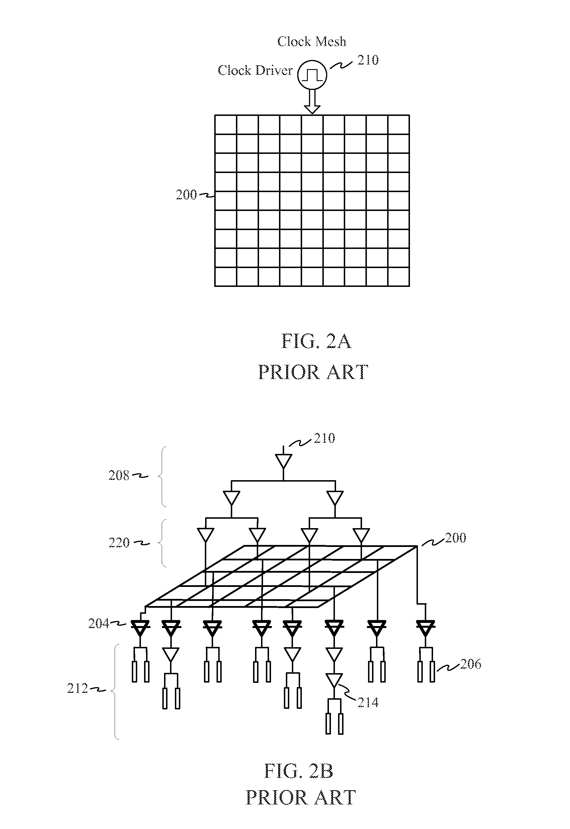
However, the use of mesh networks 200 for clock distribution increases routing overhead and substantially increases capacitance.
The increased capacitance of a mesh network 200 hinders efforts to improve clock speeds and can be a limiting factor in the development of devices with high-GHz clock speeds.
System-on-chip (SOC) clock speed are currently limited to a few GHz, for example.
Power consumption and clock skew are significant factors that limit the scaling of integrated circuits.

Method used


Image

  • Clock distribution using MTJ sensing
  • Clock distribution using MTJ sensing
  • Clock distribution using MTJ sensing

Examples


Embodiment Construction

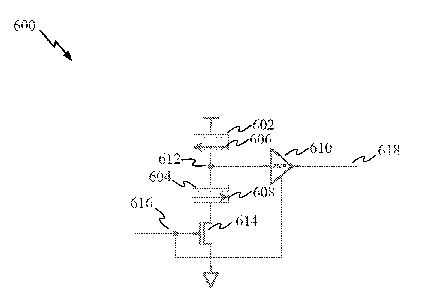
[0028]According to aspects of the present disclosure, clock signals are distributed to clocked circuits, such as logic gates on a chip, by applying an oscillating magnetic field to at least portions of the chip. Clock generation circuitry is coupled to one or more of the clocked circuits. The clock generation circuitry may be located proximately with clocked circuits on the chip to reduce clock skew. In one aspect, the clock generation circuitry includes one or more magnetic field sensing devices, such as magnetic tunnel junctions (MTJs). The clock generation circuitry is configured to generate a local clock signal in response to the oscillating magnetic field. This eliminates the need for a conventional clock distribution network and thereby reduces skew and power consumption related to the conventional clock distribution network.

[0029]Referring to FIG. 3, a clock distribution apparatus 300 according to aspects of the present disclosure includes a number of clock generation circuit...


PUM


Abstract

Clock signals are distributed on a chip by applying an oscillating magnetic field to the chip. Local clock generation circuits including magnetic field sensors are distributed around the chip and are coupled to local clocked circuitry on the chip. The magnetic field sensors may include clock magnetic tunnel junctions (MTJs) in which a magnetic orientation of the free layer is free to rotate in the free layer plane in response to the applied magnetic field. The MTJ resistance alternates between a high resistance value and a low resistance value as the free layer magnetization rotates. Clock generation circuitry coupled to the clock MTJs senses voltage oscillations caused by the alternating resistance of the clock MTJs. The clock generation circuitry includes amplifiers, which convert the sensed voltage into local clock signals.

Description

TECHNICAL FIELD[0001]The present disclosure generally relates to magnetic tunnel junction (MTJ) devices. More specifically, the present disclosure relates to MTJ sensing of distributed clock signals.BACKGROUND[0002]A significant amount of power is consumed by clock distribution networks that provide clock signals to numerous clocked circuits of systems on chip (SOC). Clock distribution networks can consume 25% to 30% of total chip power in current high speed CPUs, for example.[0003]To reduce clock skew, clock distribution networks are generally configured in a tree or mesh structure. Referring to FIG. 1A, clock distribution networks can be configured in a tree structures, commonly referred to as an H-tree structure 100 coupled to a clock source 110. The H-tree structure 100 includes a number of uniformly distributed branches 102. Referring to FIG. 1B, branches 102 of an H-tree structure 100 are coupled to respective gated buffers shown as clock gaters 114. The clock gaters 114 coupl...

Claims


Application Information

Patent Timeline
Patent Type & Authority Patents(United States)
IPC IPC(8): H03K3/00G06F1/04
CPCH03K3/59
Inventor WU, WENQINGYUEN, KENDRICK H.HANSQUINE, DAVID W.GILMORE, ROBERT P.LEVIN, JEFF A.
Owner QUALCOMM INC
Learn More