
Thin film temperature measurement using optical absorption edge wavelength

a thin film and wavelength technology, applied in the direction of optical radiation measurement, semiconductor/solid-state device testing/measurement, instruments, etc., can solve the problems of affecting the efficiency of the detector, achieving a very narrow window of temperature, and spreading the size distribution of quantum dots, so as to achieve precise, real-time measurement

Active Publication Date: 2014-07-22
K SPACE ASSOCS
View PDF23 Cites 5 Cited by
  • Summary
  • Abstract
  • Description
  • Claims
  • Application Information

AI Technical Summary

Benefits of technology

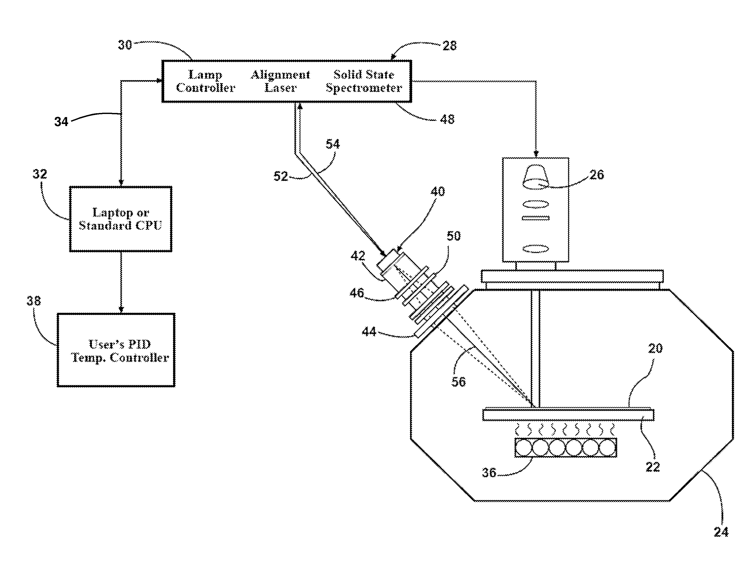
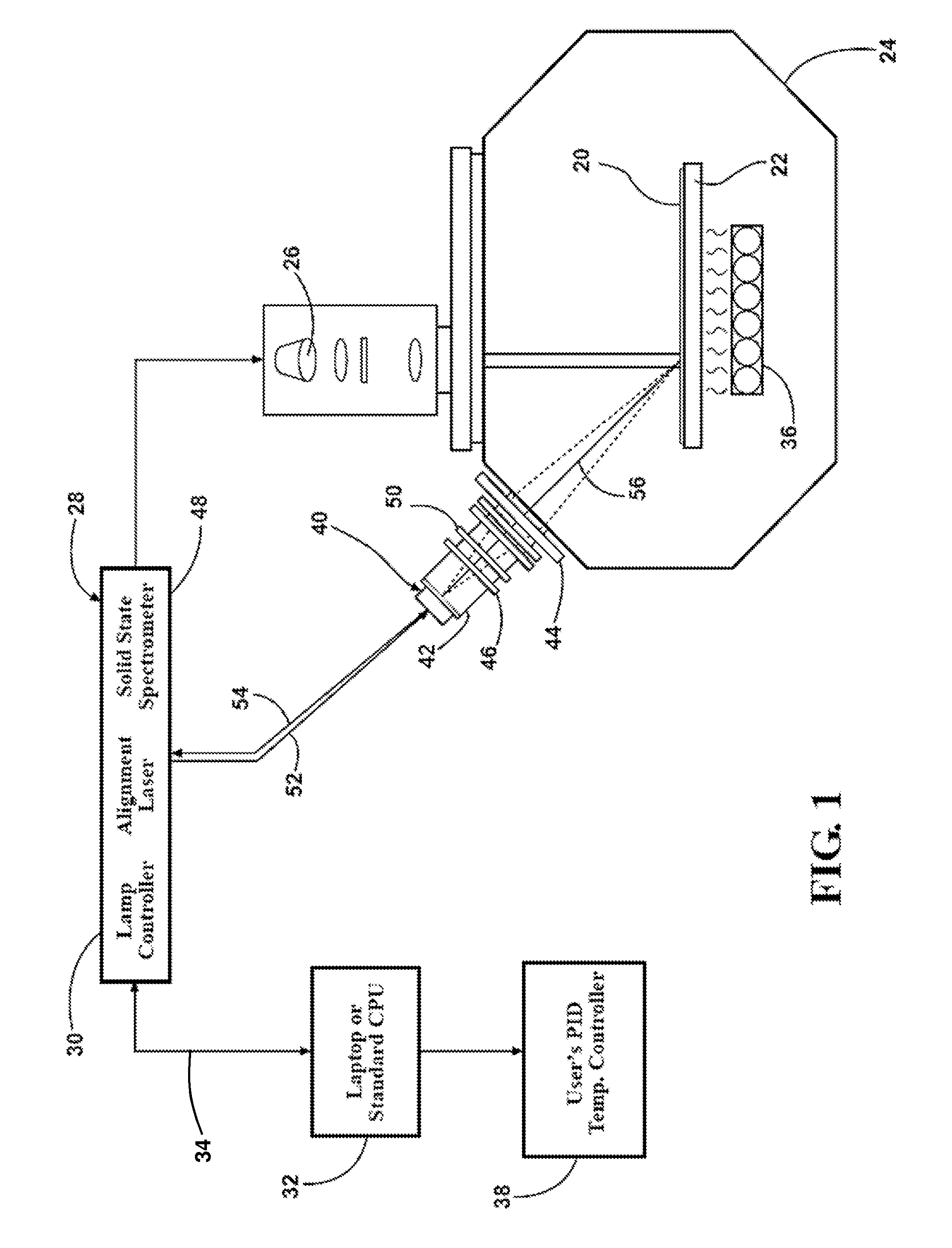
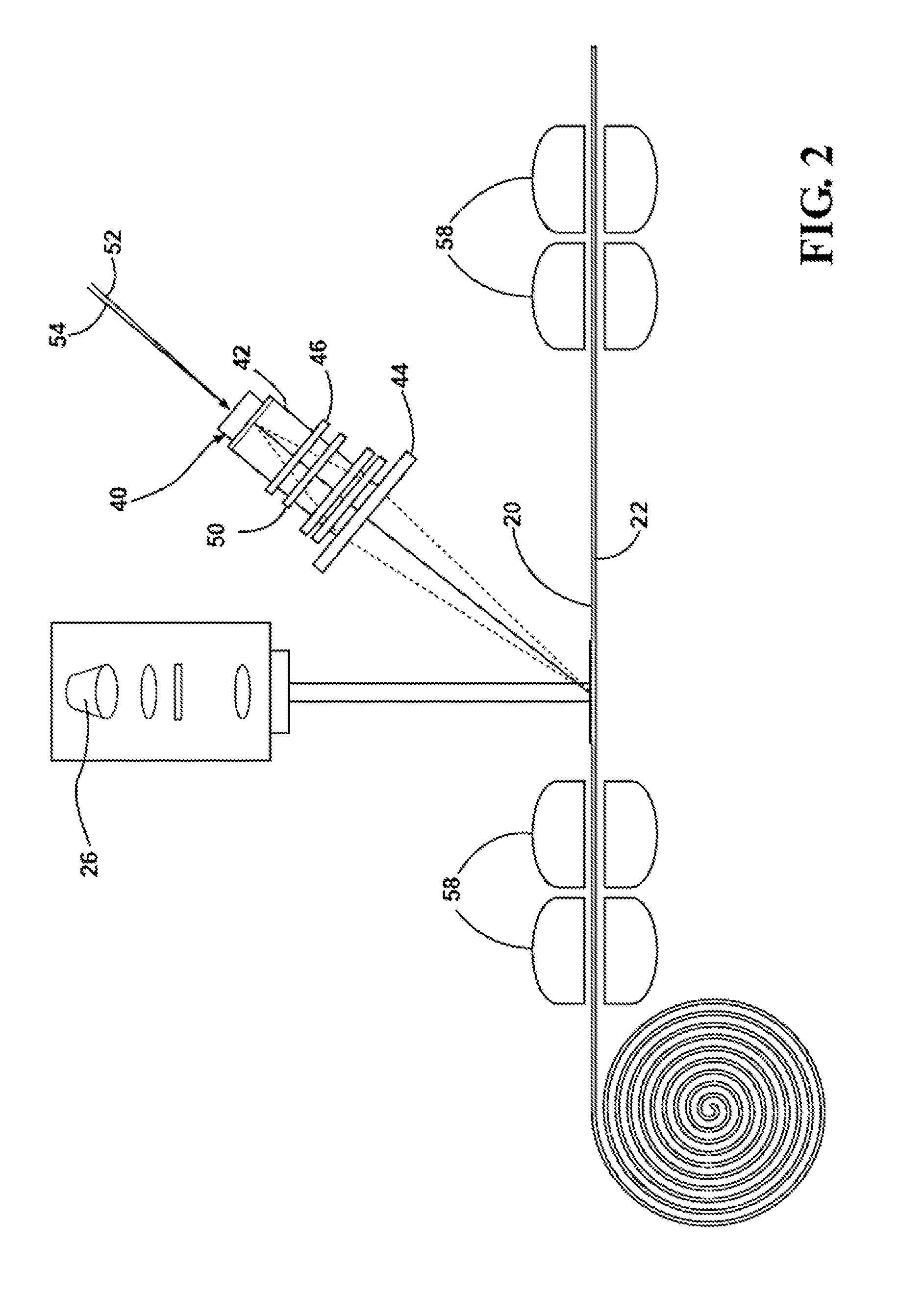
[0026]The invention provides a real-time measurement of a property having a dependence on film thickness, such as temperature of the film, when the film has a measurable optical absorption edge and the substrate has no measurable optical absorption edge. The invention takes advantage of the fact that the film is formed of a semiconductor material and thus provides a measurable optical absorption edge wavelength. By accounting for the dependence of the optical absorption edge wavelength of the film on the film thickness, the invention can provide a precise, real-time measurement of the temperature of the sample.

Problems solved by technology

This can only be accomplished in a very narrow window of temperature.
Temperature uncertainties can result in spreading of the size distribution of the quantum dots, which is detrimental to the efficiency of the detector.
One simple, but largely ineffective approach has been the use of conventional thermocouples placed in proximity to, or in direct contact with the substrate during the thin film growth operation.
This methodology is deficient in many respects, most notably, the slow response of typical thermocouples, the tendency of thermocouples (as well as other objects within the deposition chamber) to become coated with the same material being deposited on the semiconductor wafer, thereby affecting the accuracy of the thermocouple, as well as the spot thermal distortion of the surface of the semiconductor wafer resulting from physical contact between the thermocouple and the substrate.
In any event, the use of thermocouples near or in contact with the substrate is largely unacceptable during most processes because of the poor accuracy achieved.
The principal difficulties with this method are that samples typically do not emit sufficient amounts of thermal radiation until they are above approximately 450° C., and semiconductor wafers are not true black body radiators.
Hence, the use of pyrometric instruments is limited to high temperatures and the technique is known to be prone to measurement error.
While this prior art technique is in some ways effective, use of optical fiber bundles, intra-chamber optics, mechanical light choppers and mechanically scanned spectrometers renders the methodology deficient in many respects.
The detected signal suffers from temporal degradation of the optics within the deposition chamber.
The mechanical components are overly susceptible to failure and the overall methodology of collecting the signal is simply too slow for real-time measurement and control applications in the industrial production environment.
The presence of optics within the deposition chamber is problematic, since the material being deposited during the coating process tends to coat all of the contents of the chamber, including the mirrors, lenses, etc.
Over time the coatings build up and significantly reduce the collection efficiency of the optics and can lead to erroneous temperature measurement.
Not only do the mechanical components fail frequently with extended use, but it is well known that gears in scanning spectrometers wear, resulting in continual shifts in the wavelength calibration.
This leads to perpetually increasing errors in temperature measurement unless the instrument is recalibrated frequently, which is a very time-consuming process.
In addition, it is well known that scanning spectrometers are quite slow, requiring anywhere from 1-5 seconds to complete a single scan.
In this case, a temperature measurement that takes 1-5 seconds to complete is by default an average temperature and it is impossible to make any type of spatially resolved measurement.
If the process chamber has many wafers rotating on a platter about a common axis, as is typical in a production deposition system, the slow response time of the prior art makes it impossible to monitor multiple wafers.
Furthermore, the prior art utilizes a quartz halogen light source with no consideration of any type of output stabilization or intensity control.
Quartz halogen lamps are known to degrade rapidly over time leading to fluctuations in the lamp output that result in measurement variations and further system downtime for lamp replacement.
The kSA BandiT system is also insensitive to changing viewport transmission, stray light sources, and signal contribution from substrate heaters.
Despite the widespread success of the kSA BandiT system, new applications are emerging in which it is difficult to measure properties of the substrate, such as temperature, due to the non-semiconductor properties of the substrate material.
Accordingly, the prior art temperature measuring techniques may not be viable in certain limited applications.

Method used


Image

  • Thin film temperature measurement using optical absorption edge wavelength
  • Thin film temperature measurement using optical absorption edge wavelength
  • Thin film temperature measurement using optical absorption edge wavelength

Examples


example 1

[0076]In one embodiment, determining the temperature of a GaN film 20 on a sapphire substrate 22 includes first generating an optical absorption edge wavelength versus thickness calibration table or curve (thickness calibration table) for a GaN film 20, as shown in FIG. 10. Next, the method includes generating an optical absorption edge wavelength versus temperature calibration table (temperature calibration table) for a GaN film 20 at a single, predetermined thickness, for example 3.0 μm, using the kSA method disclosed in Publication No. 2005 / 0106876 and U.S. Publication No. 2009 / 0177432. The thickness calibration table at 3.0 μm and temperature calibration table is incorporated into the software program, which can be provided to a customer. The calibration tables are used to determine the temperature of a GaN film at other thicknesses. For example, the temperature of a film having a thickness of 4.0 μm is determined by producing a spectra at 4.0 μm. The optical absorption edge wav...

example 2

[0077]The method of the present invention can be implemented in the software program installed in the computer 32 of the apparatus and system described above. The kSA BandiT system, discussed in US Publication No. 2005 / 0106876 and U.S. Publication No. 2009 / 0177432 can be modified to include the method of the present invention.

[0078]The software program determines the film thickness using the spectra and Equation 2, discussed above. The step of determining the thickness of the film requires inputting several parameters, as shown in FIG. 11. The first parameter is the number of slopes, which is defined as the required number of slopes detected in succession that have at least the minimum slope defined by the user. The parameters also include minimum slope, which is defined as the minimum slope required to deem a peak or valley as real and not noise; boxcar width, which is defined as the amount of boxcar smoothing of the raw spectra; minimum wavelength, which is defined as the lowest w...


PUM

PropertyMeasurementUnit
temperatureaaaaaaaaaa
thicknessaaaaaaaaaa
thicknessaaaaaaaaaa

Abstract

A technique for determining the temperature of a sample including a semiconductor film 20 having a measurable optical absorption edge deposited on a transparent substrate 22 of material having no measurable optical absorption edge, such as a GaN film 20 deposited on an Al2O3 substrate 22 for blue and white LEDs. The temperature is determined in realtime as the film 20 grows and increases in thickness. A spectra based on the diffusely scattered light from the film 20 is produced at each incremental thickness. A reference division is performed on each spectra to correct for equipment artifacts. The thickness of the film 20 and an optical absorption edge wavelength value are determined from the spectra. The temperature of the film 20 is determined as a function of the optical absorption edge wavelength and the thickness of the film 20 using the spectra, a thickness calibration table, and a temperature calibration table.

Description

CROSS REFERENCE TO RELATED APPLICATIONS[0001]This application claims priority to Provisional Patent Application No. 61 / 218,523, filed Jun. 19, 2009, the entire disclosures of which is hereby incorporated by reference and relied upon.BACKGROUND OF THE INVENTION[0002]1. Field of the Invention[0003]The invention relates generally to methods for making precise non-contact measurements of substrate and thin film temperature during growth and processing of the thin film on the substrate.[0004]2. Related Art[0005]Advanced manufacturing processes involving depositing thin films on substrates often depend on the ability to monitor and control a property of the substrate, such as temperature, with high precision and repeatability.[0006]For many applications, precise temperature measurement during the growth of a thin film on a semiconductor wafer or substrate is critical to the ultimate quality of the finished, coated wafer and in turn to the performance of the opto-electronic devices constru...

Claims


Application Information

Patent Timeline
Patent Type & Authority Patents(United States)
IPC IPC(8): G01N21/00G01N21/47
CPCH01L21/67248H01L22/12
Inventor BARLETT, DARRYLTAYLOR, II, CHARLES A.WISSMAN, BARRY D.
Owner K SPACE ASSOCS
Learn More