Bipolar stacked transistor architecture

a technology of bipolar transistors and transistors, applied in the direction of amplifiers with multiple amplifiers, amplifiers with semiconductor devices only, amplifiers with semiconductor devices, etc., can solve the problems of reducing rf output power, reducing the distance between transmitters, and remained expensive, so as to prevent the breakdown of bipolar devices and reduce the negative rf feedback to amplifiers.

Active Publication Date: 2014-07-29
GEORGE WASHINGTON UNIVERSITY +1
View PDF9 Cites 6 Cited by
  • Summary
  • Abstract
  • Description
  • Claims
  • Application Information

AI Technical Summary

Benefits of technology

[0014]The circuit configuration includes: (4) The use of bipolar transistor devices over field effect transistor (FET) devices used in present technology. (5) The use of a ratioed-current mirror to provide: DC bias, prevent breakdown of the bipolar devices in the main stack, and provide negative RF feedback to the amplifiers.

Problems solved by technology

However, due to low volume production, they have also remained expensive.
Silicon-based integrated circuit technologies, long dominant in the digital computer industry, have enjoyed inexpensive production costs due to the mass volume of production.
While silicon-based integrated circuits are essentially ‘as fast as’ III-V-based integrated circuits, because they are optimized for digital behavior and not analog behavior as III-V-based technologies are, they do not match III-V's in terms of a second key metric: RF output power.
However, with the recent allocations made by the FCC, large research efforts have been undertaken to use commercially available, low cost silicon-based integrated circuit technology for millimeter-wave communications over high cost III-V-based integrated circuit technology.
When an integrated circuit technology that incapable of generating large amounts of RF output power to create the transmitter's power amplifier, the transmitter will have a limited distance that it can ‘transmit’ the broadcast signal.
For a transmitter's power amplifiers made from such devices, this results in reduced RF output power and requires more complex circuitry to allow it to operate in a transmitter / receiver system.
A commonly used technique to increase RF output power is to place transistors in parallel, which increases the output current swing of an amplifier, but reduces the output impedance.
This makes input and output impedance matching more difficult for the designer.

Method used


Image

  • Bipolar stacked transistor architecture
  • Bipolar stacked transistor architecture
  • Bipolar stacked transistor architecture

Examples


Embodiment Construction

[0030]In describing the preferred embodiments of the present invention illustrated in the to drawings, specific terminology is resorted to for the sake of clarity. However, the present invention is not intended to be limited to the specific terms so selected, and it is to be understood that each specific term includes all technical equivalents that operate in a similar manner to accomplish a similar purpose.

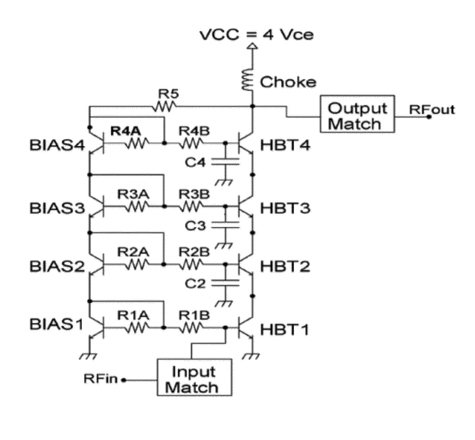
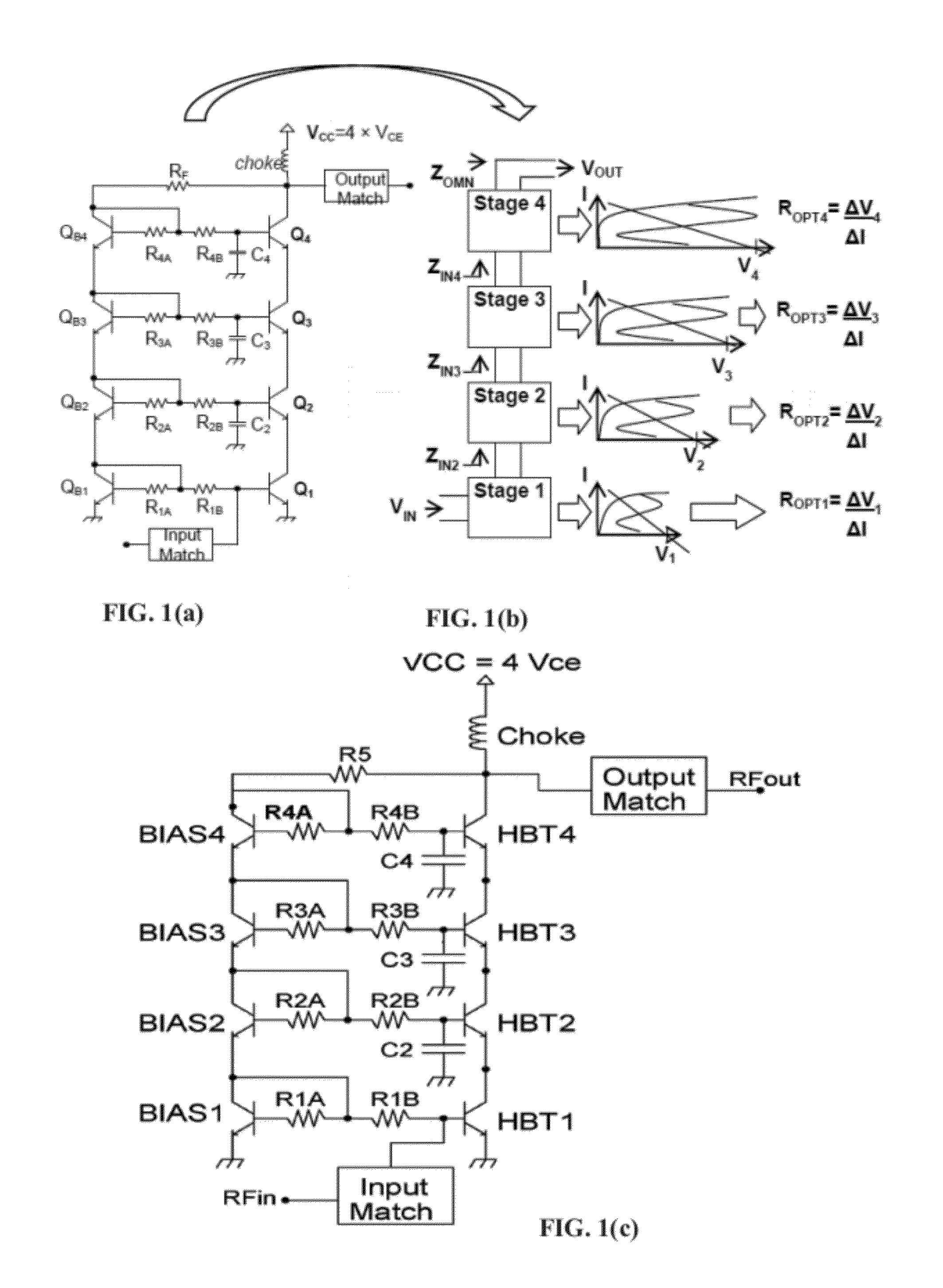
[0031]The implementation of FIGS. 1(a), (b) use a stack of four Bipolar Transistors, Q1-Q4. Q1-Q4 are identical in emitter area size. The supply voltage (VCC) is set to four times a single transistor's supply voltage (VCE) or bias value. The Bipolar transistor labeled QB1, along with resistors R1A and R1B, serves as a ratioed current mirror for bipolar transistor Q1; this is true for QB2-4 for Q2-Q4 as well. Resistor labeled: RF serves a dual purpose: negative feedback and variable DC bias control. As the RF output signal swings up and down, resistor, RF changes the reference cur...


PUM


Abstract

An amplifier for an integrated circuit has a plurality of ratioed current mirrors connected to each other in a stacked configuration. Each ratio mirror has at least two resistors and at least two bipolar transistors connected to each other via said at least two resistors. Each amplifying transistor, contains a capacitor, and potentially and inductor, to internally match the transistors that make up the amplifying stack. DC, harmonic and s-parameter simulations are performed to provide an optimal impedance for each of the stacked transistors to maximize the RF power output of each stacked layer and the amplifier.

Description

RELATED APPLICATIONS[0001]This application claims the benefit of U.S. Provisional Application No. 61 / 466,244, filed Mar. 22, 2011, the entire content of which is incorporated herein by reference.BACKGROUND OF THE INVENTION[0002]1. Field of the Invention[0003]The present invention relates to a transistor architecture and simulation technique for optimizing the transistor architecture. More particularly, the present invention is for an architecture having stacked bipolar transistors for a high power amplifier, and a simulation technique for maximizing the transistor RF power output.[0004]2. Background of the Related Art[0005]Recently, the FCC has made several large commercially available allocations of the bandwidth in the millimeter-wave communication bands, namely the V-band (59-64 GHz), E-bands (71-76 GHz & 81-86 GHz), and the W-band (92-95 GHz). Integrated circuit technology that is both mature and capable of operating at these very high millimeter-wave frequencies is known as III...

Claims


Application Information

Patent Timeline
Patent Type & Authority Patents(United States)
IPC IPC(8): H03F3/04
CPCH03F2200/18H03F2200/72H03F3/42H03F3/19H03F1/0266H03F2200/168H03F1/34
Inventor DARWISH, ALIFARM, THOMAS J.ZAGHLOUL, MONA
Owner GEORGE WASHINGTON UNIVERSITY
Why Eureka
Try Eureka