Apparatus for and method of wafer edge exposure
a technology of wafer edge and apparatus, applied in the field of apparatus for and a method of wafer edge exposure, can solve the problems of increasing the size of patterns, single light source, and inability to properly expose undesired photoresist film
- Summary
- Abstract
- Description
- Claims
- Application Information
AI Technical Summary
Benefits of technology
Problems solved by technology
Method used
Image

Examples
Embodiment Construction
[0023]Reference will now be made in detail to the present examples of the invention illustrated in the accompanying drawings. Wherever possible, the same reference numbers will be used throughout the drawings to refer to the same or like portions. It should be noted that the drawings are in greatly simplified form and are not to precise scale.
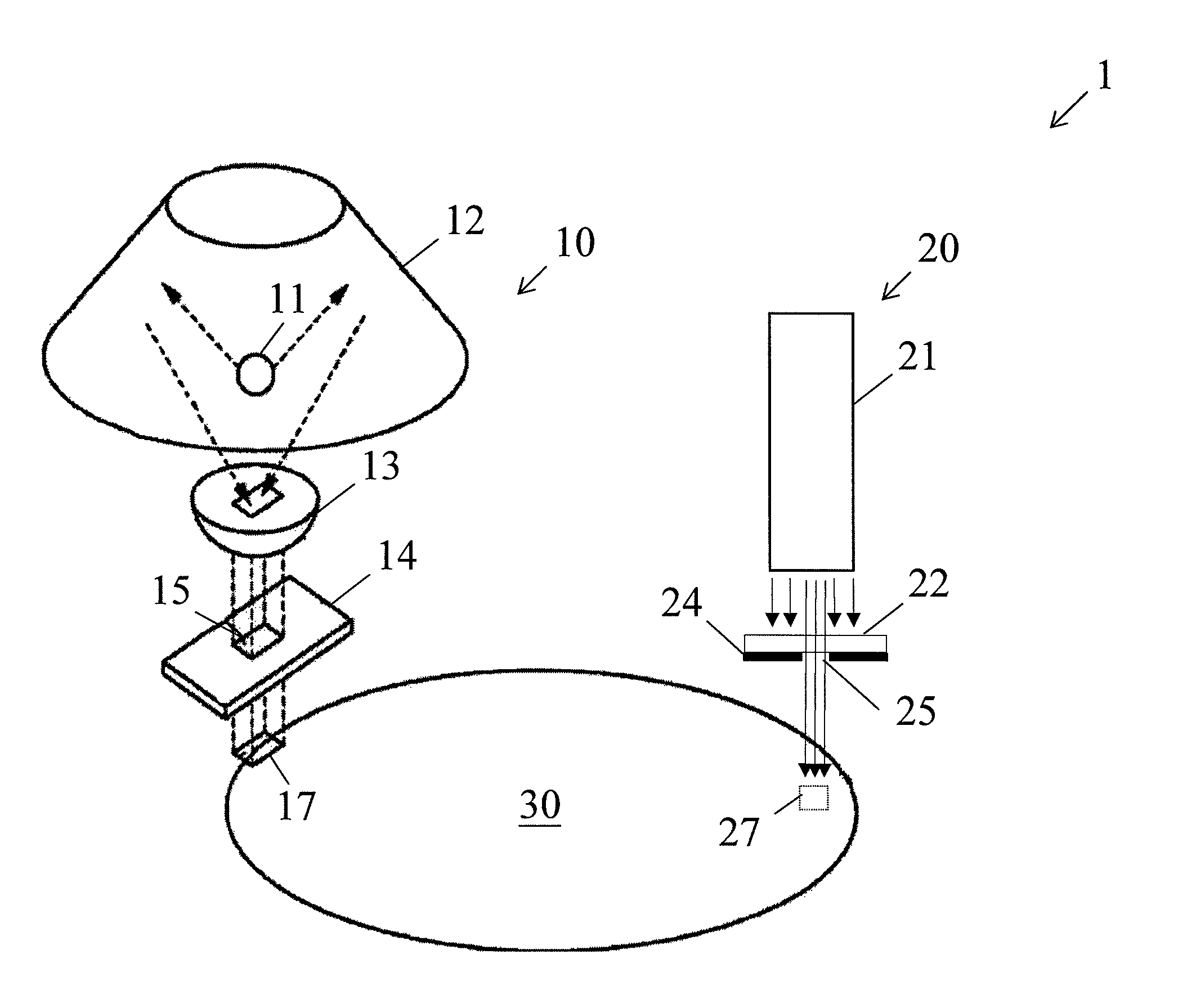
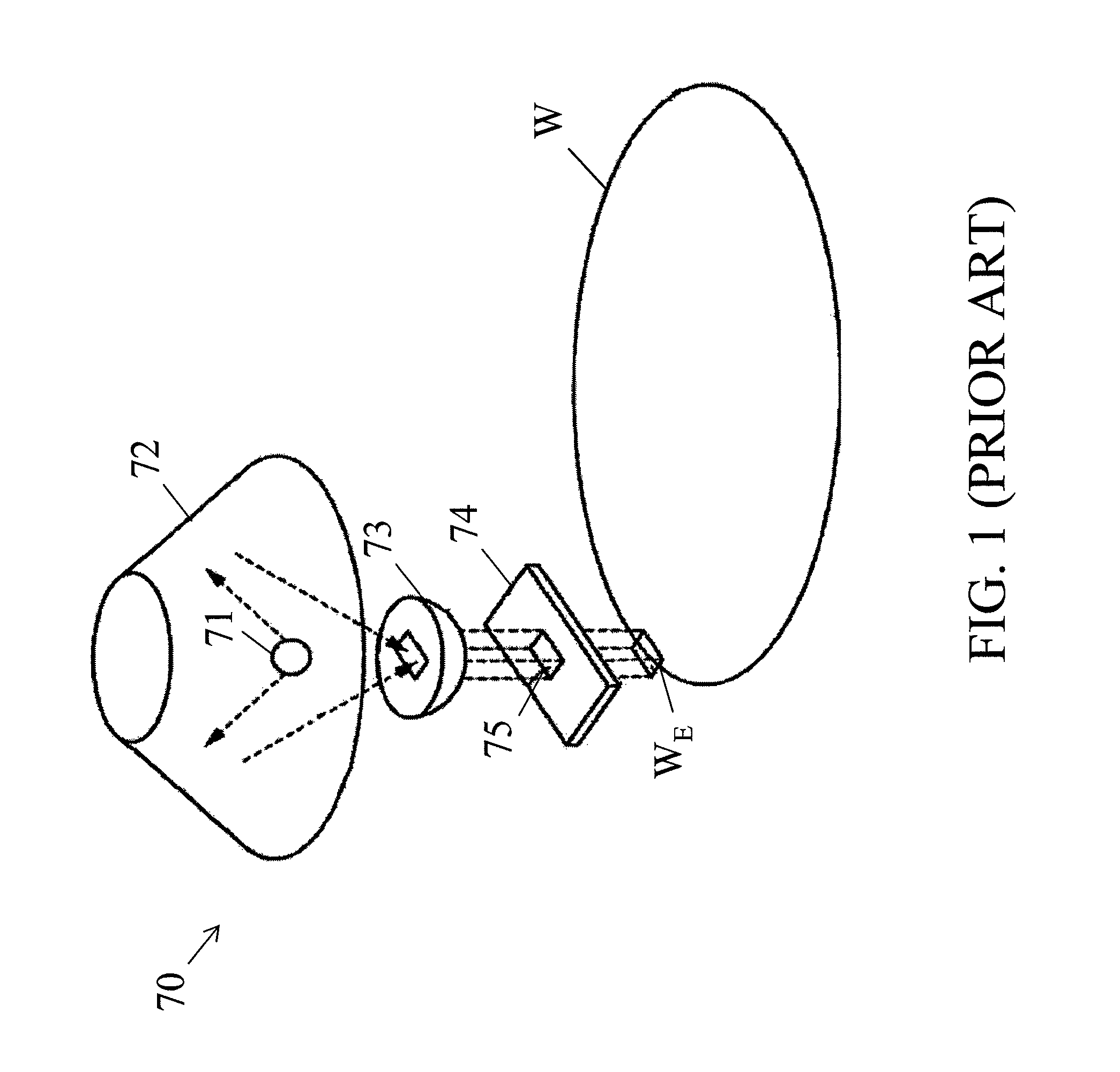
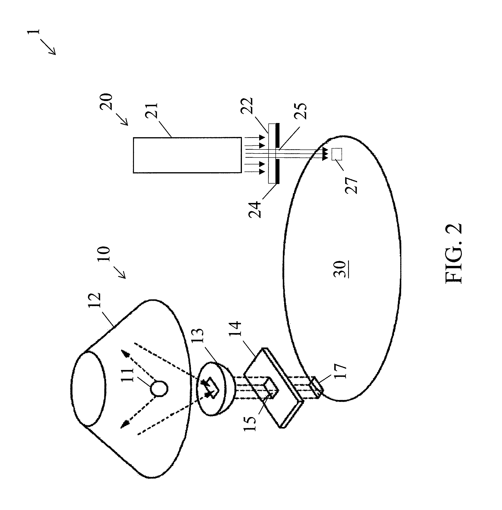
[0024]FIG. 2 is a schematic diagram of an apparatus 1 for wafer edge exposure (WEE) in accordance with an example of the present invention. To expose a wafer, the apparatus 1 may work in conjunction with a photolithography apparatus. However, for simplicity, only the apparatus 1 for wafer edge exposure is illustrated and the photolithography apparatus or other is omitted.
[0025]Referring to FIG. 2, the apparatus 1 may include a first exposure unit 10 and a second exposure unit 20. The first exposure unit 10 may further include a first light source 11, a reflector 12, a collective lens 13 and a first mask 14 with a first opening 15 for performing...
PUM
 Abstract
Description
Claims
Application Information
 - R&D
- Intellectual Property
- Life Sciences
- Materials
- Tech Scout
- Unparalleled Data Quality
- Higher Quality Content
- 60% Fewer Hallucinations
Browse by: Latest US Patents, China's latest patents, Technical Efficacy Thesaurus, Application Domain, Technology Topic, Popular Technical Reports.
© 2025 PatSnap. All rights reserved.Legal|Privacy policy|Modern Slavery Act Transparency Statement|Sitemap|About US| Contact US: help@patsnap.com