Organic light emitting display

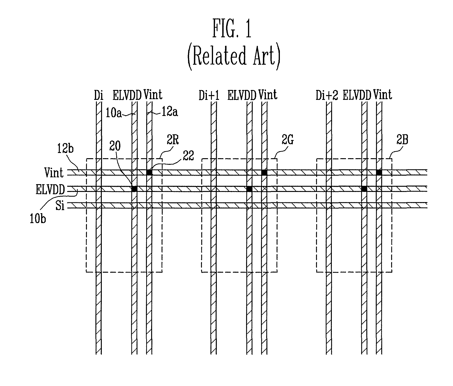
a light-emitting display and organic technology, applied in static indicating devices, instruments, thermoelectric devices, etc., can solve the problems of complex layout structure, difficult to manufacture all transistors of organic light-emitting displays to have the same properties using current manufacturing technologies, and non-uniform display, etc., to achieve simplified wiring line structure and reduce the number of wiring lines

Active Publication Date: 2014-08-26
SAMSUNG DISPLAY CO LTD
View PDF16 Cites 9 Cited by
  • Summary
  • Abstract
  • Description
  • Claims
  • Application Information

AI Technical Summary

Benefits of technology

[0017]Accordingly, an aspect of embodiments according to the present invention provides an organic light emitting display capable of reducing or minimizing the number of wiring lines to improve an aperture ratio.
[0029]In the organic light emitting display according to embodiments of the present invention, since one first power source line is provided for every at least two data lines, the number of wiring lines may be reduced or minimized. In addition, in the first power source lines, a first group of first power source lines receives a first power source and the second group of first power source line receives a power source different from the first power source. That is, according to embodiments of the present invention, at least two power sources may be supplied to sub pixels using the first power source lines separated from each other by substantially the same distance so that a wiring line structure may be simplified.

Problems solved by technology

In an organic light emitting display, an amount of current that flows to the OLED varies with the threshold voltage variation of the driving transistor included in each of the pixels and non-uniform displaying may therefore occur.
That is, properties of the driving transistor, such as its threshold voltage, vary with the manufacturing process of the driving transistor included in each of the pixels, making it very difficult to manufacture all transistors of the organic light emitting display to have the same properties using current manufacturing technologies.
However, since each of the above sub pixels 2R, 2G, and 2B is coupled to six wiring lines, a layout structure is complicated and an aperture ratio is reduced.

Method used


Image

  • Organic light emitting display
  • Organic light emitting display
  • Organic light emitting display

Examples


Embodiment Construction

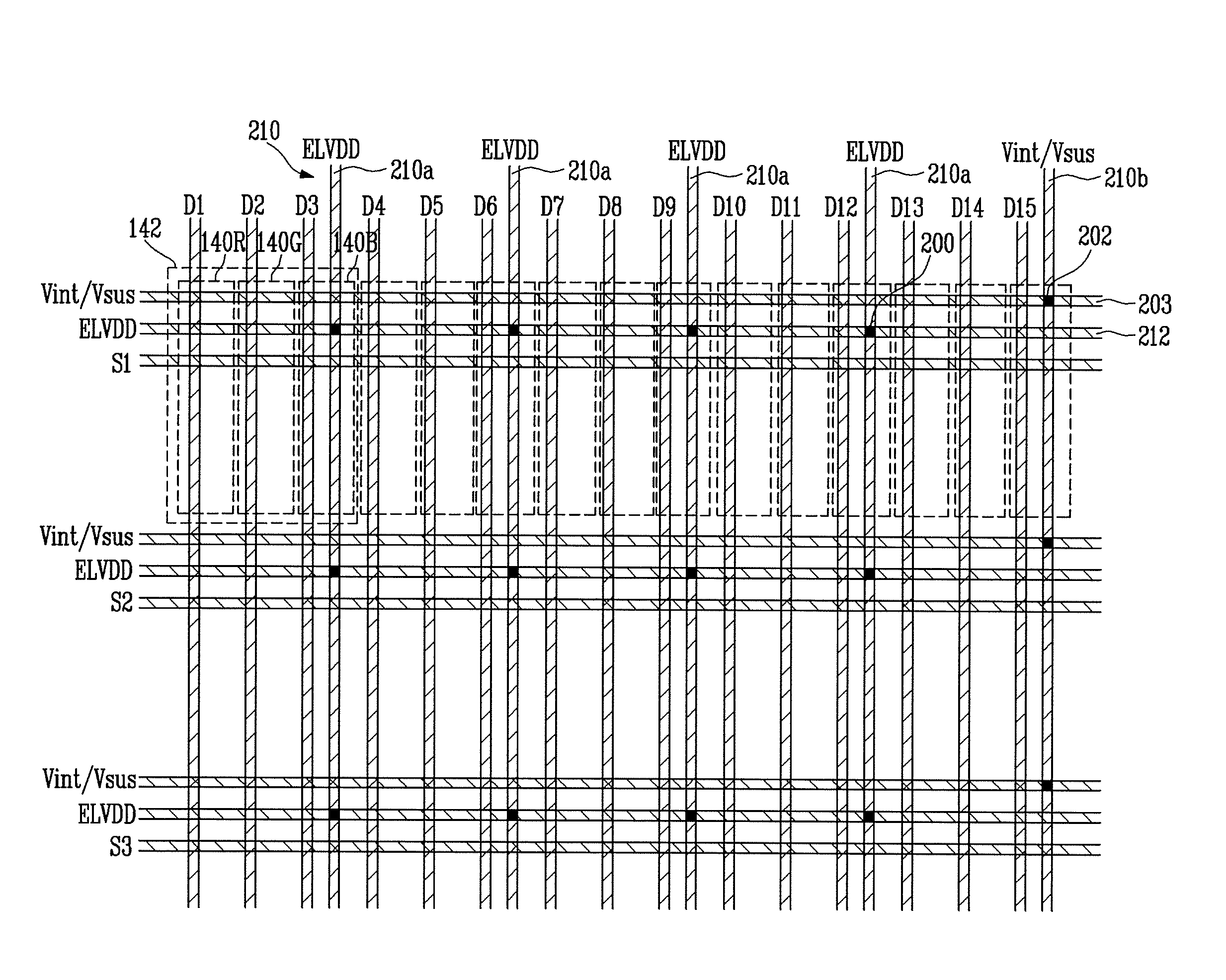
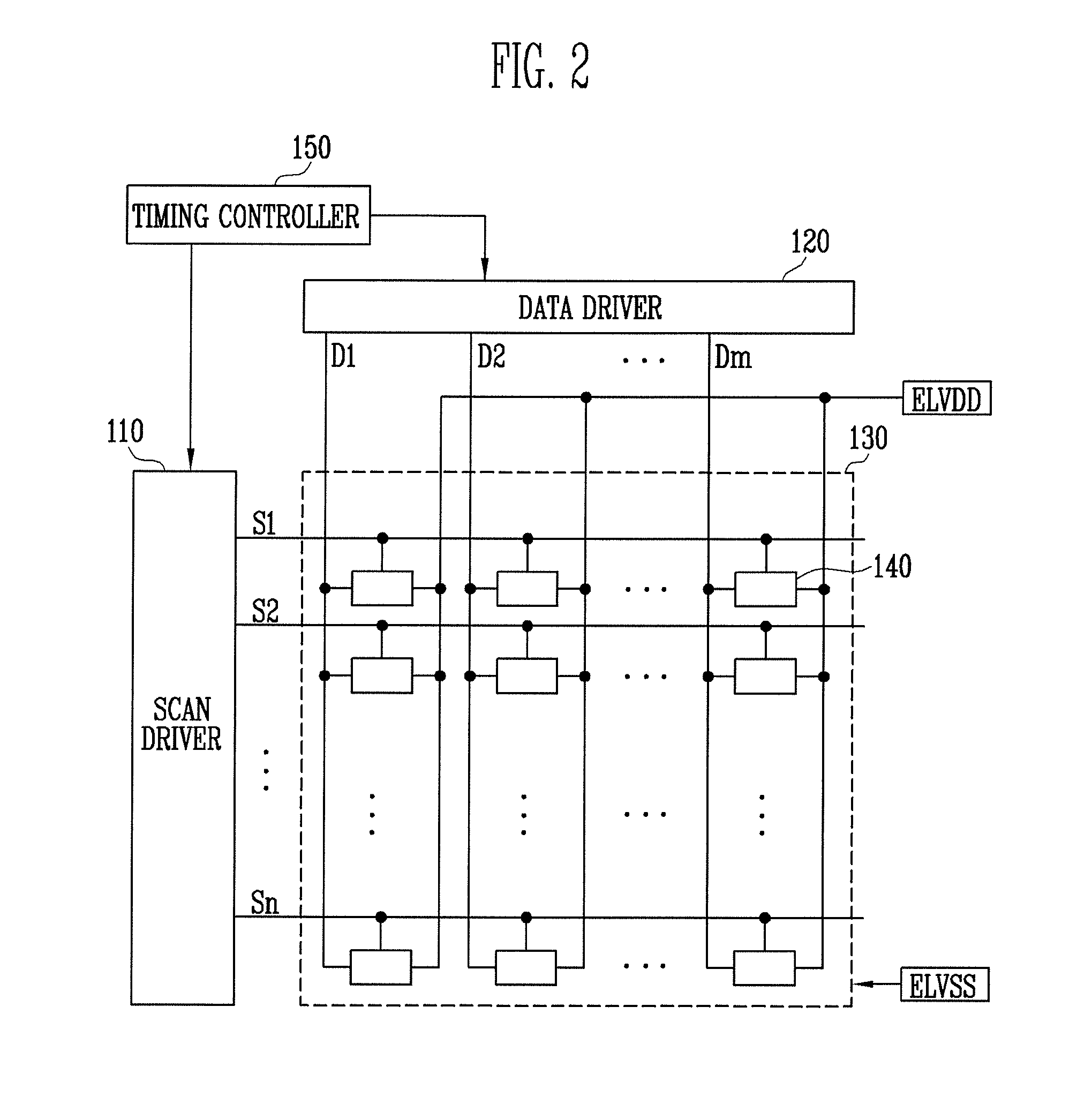
[0034]Hereinafter, certain exemplary embodiments according to the present invention will be described with reference to the accompanying drawings. Here, when a first element is described as being coupled to a second element, the first element may be directly coupled to the second element or may be indirectly coupled to the second element via one or more other elements. Further, some of the elements that are not essential to a complete understanding of the invention are omitted for clarity. Also, like reference numerals refer to like elements throughout. The embodiments of the present invention may have different forms, and should not be construed as being limited to the descriptions set forth herein. Accordingly, hereinafter the exemplary embodiments by which those skilled in the art may perform the present invention are described in detail with reference to FIGS. 2 and 3 to merely explain aspects of embodiments according to the present invention.

[0035]FIG. 2 is a view illustrating ...


PUM


Abstract

An organic light emitting display is capable of reducing or minimizing the number of wiring lines to improve an aperture ratio. The organic light emitting display includes scan lines and data lines that cross each other at crossing regions, sub pixels located at the crossing regions that display an image in accordance with an amount of current that flows from a first power source to respective organic light emitting diodes in the sub pixels, and first power source lines that are parallel to the data lines, each of the first power source lines corresponding to at least two of the data lines. The first power source lines include a first group of the first power source lines that receive the first power source and a second group of the first power source lines that receive a second power source.

Description

CROSS-REFERENCE TO RELATED APPLICATION[0001]This application claims priority to and the benefit of Korean Patent Application No. 10-2010-0023761, filed on Mar. 17, 2010, in the Korean Intellectual Property Office, the entire content of which is incorporated herein by reference.BACKGROUND[0002]1. Field[0003]One or more embodiments of the present invention relate to an organic light emitting display.[0004]2. Description of Related Art[0005]Recently, various flat panel displays (FPDs) capable of reducing weight and volume that are disadvantages of cathode ray tubes (CRTs) have been developed. The FPDs include liquid crystal displays (LCDs), field emission displays (FEDs), plasma display panels (PDPs), organic light emitting displays, and the like.[0006]Among the FPDs, the organic light emitting display displays images using organic light emitting diodes (OLEDs) that generate light by the recombination of electrons and holes. The organic light emitting display has advantages of a high r...

Claims


Application Information

Patent Timeline
Patent Type & Authority Patents(United States)
IPC IPC(8): H01L51/52
CPCH01L27/3276H10K59/131
Inventor CHOI, SANG-MOO
Owner SAMSUNG DISPLAY CO LTD
Why Eureka
Try Eureka