Semiconductor device

a technology of semiconductors and transistors, applied in the direction of semiconductor devices, electrical equipment, transistors, etc., can solve the problems of difficult to increase the on-state current of the transistor, the technique of valence electron control with the addition of impurities has not been established, etc., and achieves the effect of large on-state current and large on-state curren

Inactive Publication Date: 2014-09-02
SEMICON ENERGY LAB CO LTD
View PDF137 Cites 5 Cited by
  • Summary
  • Abstract
  • Description
  • Claims
  • Application Information

AI Technical Summary

Benefits of technology

[0008]In view of the above-described technical background, an object of one embodiment of the invention is to provide a semiconductor device that can increase the on-state current of a transistor.
[0010]According to one embodiment of the invention, the gap between the source electrode and the drain electrode in a direction in which carriers transfer in the semiconductor film, i.e., the channel length direction, can be determined by the gap between the pair of first conductive films. Accordingly, the pair of second conductive films can be positioned such that the gap between the pair of second conductive films is longer than that between the pair of first conductive films. Therefore, according to one embodiment of the invention, in the case where the gap between the source electrode and the drain electrode needs to be short in order to miniaturize the transistor, the gap between the pair of first conductive films may be short, and the gap between the pair of second conductive films can be long so that the pair of second conductive films does not overlap with the third conductive film over the semiconductor film. Specifically, over the semiconductor film, the third conductive film can be interposed between the pair of second conductive films and be away from the pair of second conductive films. Accordingly, even when the transistor is miniaturized, an electric field applied to the semiconductor film from the third conductive film is unlikely to be interrupted by the pair of second conductive films, resulting in large on-state current.
[0011]Further, according to one embodiment of the invention, the pair of first conductive films exists below the semiconductor film, and the third conductive film exists over the semiconductor film. Accordingly, even when the third conductive film functioning as the gate electrode overlaps with the pair of first conductive films owing to miniaturization of the transistor with the gap between the pair of first conductive films being short, the electric field applied to the semiconductor film from the third conductive film is unlikely to be interrupted by the pair of first conductive films. As a result, even when the transistor is miniaturized, large on-state current can be obtained.
[0012]Further, even when the thickness of each of the pair of first conductive films is made small in order to enhance the step coverage with the semiconductor film in end portions of the pair of first conductive films, the resistance of the source electrode and the drain electrode, which are formed using the pair of first conductive films and the pair of second conductive films, can be suppressed to be low because one of the pair of first conductive films and the other of the pair of first conductive films are connected to one of the pair of second conductive films and the other of the pair of second conductive films, respectively.
[0014]In the case where the pair of second conductive films is located over the semiconductor film, the pair of first conductive films and the pair of second conductive films which function as the source electrode and the drain electrode can have a larger area that is in contact with the semiconductor film than in the case where the pair of second conductive films is away from the semiconductor film. Accordingly, even when the transistor is miniaturized, the contact resistance between the semiconductor film and source electrode and the drain electrode which are formed using the pair of first conductive films and the pair of second conductive films can be suppressed to be low, resulting in large on-state current.
[0015]According to one embodiment of the invention, any of the above-described structures can achieve a semiconductor device including a transistor with large on-state current.

Problems solved by technology

However, in a transistor formed using an oxide semiconductor, unlike in the transistor formed using silicon, the technique of valence electron control with the addition of impurity has not been established yet.
Therefore, ensuring the step coverage makes it difficult to increase the on-state current of the transistor.

Method used


Image

  • Semiconductor device
  • Semiconductor device
  • Semiconductor device

Examples


embodiment 1

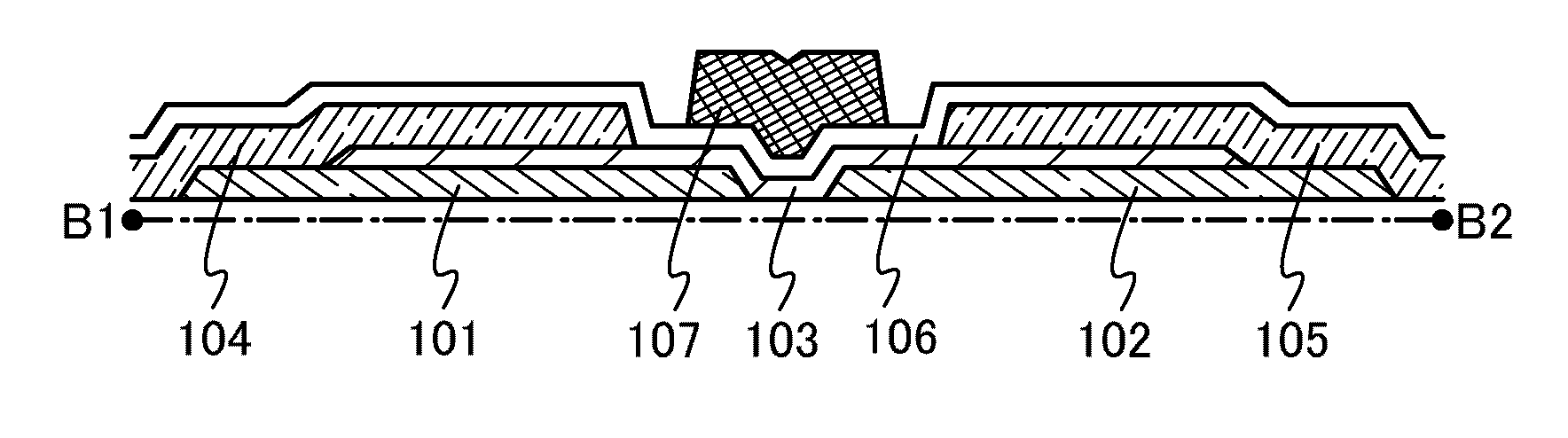
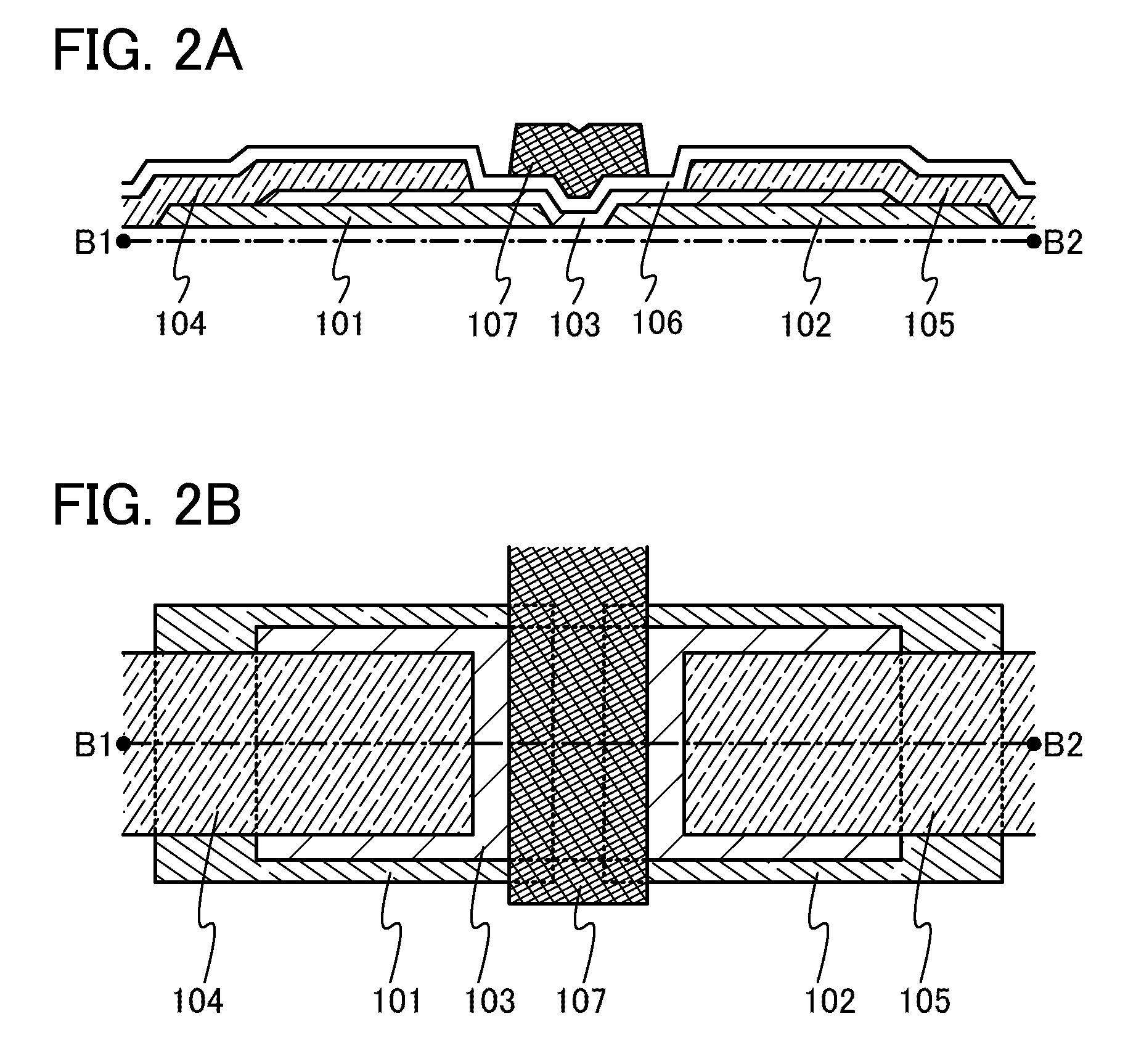
[0030]FIGS. 1A to 1C illustrate examples of a structure of a transistor included in a semiconductor device according to one embodiment of the invention. FIG. 1A is an example of a cross-sectional view of the transistor in the channel length direction.

[0031]The transistor in FIG. 1A includes, over an insulating surface, a first conductive film 101 and a first conductive film 102, a semiconductor film 103 over the first conductive film 101 and the first conductive film 102, a second conductive film 104 and a second conductive film 105 which are connected to the first conductive film 101 and the first conductive film 102, respectively, an insulating film 106 over the semiconductor film 103, and a third conductive film 107 provided in a position overlapping with the semiconductor film 103 over the insulating film 106 between the second conductive film 104 and the second conductive film 105.

[0032]The first conductive film 101 and the second conductive film 104 function as one of a source...

embodiment 2

[0089]The semiconductor device according to one embodiment of the invention may have a structure in which transistors are stacked. In particular, a transistor having the structure in FIG. 4A can be used such that the fourth conductive film 110 or the fourth conductive film 111 functions as any of a gate electrode, a source electrode, and a drain electrode of a transistor in a lower layer. Accordingly, the semiconductor device can be miniaturized with an increase in element area due to contact area suppressed, or the number of steps for manufacturing the transistor can be reduced.

[0090]This embodiment shows a method of manufacturing the semiconductor device according to one embodiment of the invention, which has a structure in which a transistor is provided below the transistor having the structure in FIG. 4A, by taking a memory device which is one of semiconductor devices as an example.

[0091]First, in advance of the description of the manufacturing method, a structure of a memory ce...

embodiment 3

[0182]A structure example of an inverter that is one of the semiconductor devices according to one embodiment of the invention is described.

[0183]FIG. 11 illustrates an example of an inverter according to one embodiment of the invention. An inverter 500 in FIG. 11 includes a transistor 501, a transistor 502, a transistor 503, a transistor 504, a transistor 505, and a capacitor 506.

[0184]A gate electrode of the transistor 501 is connected to a wiring 508; a source electrode of the transistor 501 is connected to a drain electrode of the transistor 502; and a drain electrode of the transistor 501 is connected to a wiring 507. A gate electrode of the transistor 502 is connected to a wiring 509; a source electrode of the transistor 502 is connected to a wiring 510; and the drain electrode of the transistor 502 is connected to the source electrode of the transistor 501. A gate electrode of the transistor 503 is connected to the wiring 507; one of a source electrode and a drain electrode o...


PUM


Abstract

Provided is a semiconductor device including a transistor with large on-state current even when it is miniaturized. The transistor includes a pair of first conductive films over an insulating surface; a semiconductor film over the pair of first conductive films; a pair of second conductive films, with one of the pair of second conductive films and the other of the pair of second conductive films being connected to one of the pair of first conductive films and the other of the pair of first conductive films, respectively; an insulating film over the semiconductor film; and a third conductive film provided in a position overlapping with the semiconductor film over the insulating film. Further, over the semiconductor film, the third conductive film is interposed between the pair of second conductive films and away from the pair of second conductive films.

Description

TECHNICAL FIELD[0001]The present invention relates to a semiconductor device using an insulated-gate field-effect transistor.BACKGROUND ART[0002]In recent years, a metal oxide having semiconductor characteristics, which is called an oxide semiconductor, has attracted attention as a novel semiconductor material having high mobility as in the case of polysilicon or microcrystalline silicon and having uniform element characteristics as in the case of amorphous silicon. The metal oxide is used for various applications. For example, indium oxide is a well-known metal oxide and used as a material of a transparent electrode included in a liquid crystal display device or the like. Examples of such metal oxides having semiconductor characteristics include tungsten oxide, tin oxide, indium oxide, and zinc oxide. Transistors in which a channel formation region is formed using such a metal oxide having semiconductor characteristics have been known (Patent Documents 1 and 2).REFERENCEPatent Docu...

Claims


Application Information

Patent Timeline
Patent Type & Authority Patents(United States)
IPC IPC(8): H01L29/10H01L27/12H01L29/786
CPCH01L29/10H01L29/7869H01L27/12H01L27/1225H01L29/41733H01L29/41775
Inventor YAMAZAKI, SHUNPEIISOBE, ATSUOSASAKI, TOSHINARI
Owner SEMICON ENERGY LAB CO LTD
Why Eureka
Try Eureka