Dielectric waveguide filter with structure and method for adjusting bandwidth

a dielectric waveguide and filter technology, applied in waveguides, resonators, electrical equipment, etc., can solve the problems of limiting the external bandwidth to unduly narrow filter bands, unpredictable filter performance,

Active Publication Date: 2014-09-02
CTS CORP ELKHART
View PDF67 Cites 24 Cited by
  • Summary
  • Abstract
  • Description
  • Claims
  • Application Information

AI Technical Summary

Problems solved by technology

The plating of blind input-output holes during the manufacturing process however has proven unreliable and can lead to unpredictable filter performance.
However, coupling with plated input / output through-holes, when used with thick waveguide filters, limits the external bandwidth to unduly narrow band filters.

Method used


Image

  • Dielectric waveguide filter with structure and method for adjusting bandwidth
  • Dielectric waveguide filter with structure and method for adjusting bandwidth
  • Dielectric waveguide filter with structure and method for adjusting bandwidth

Examples


Embodiment Construction

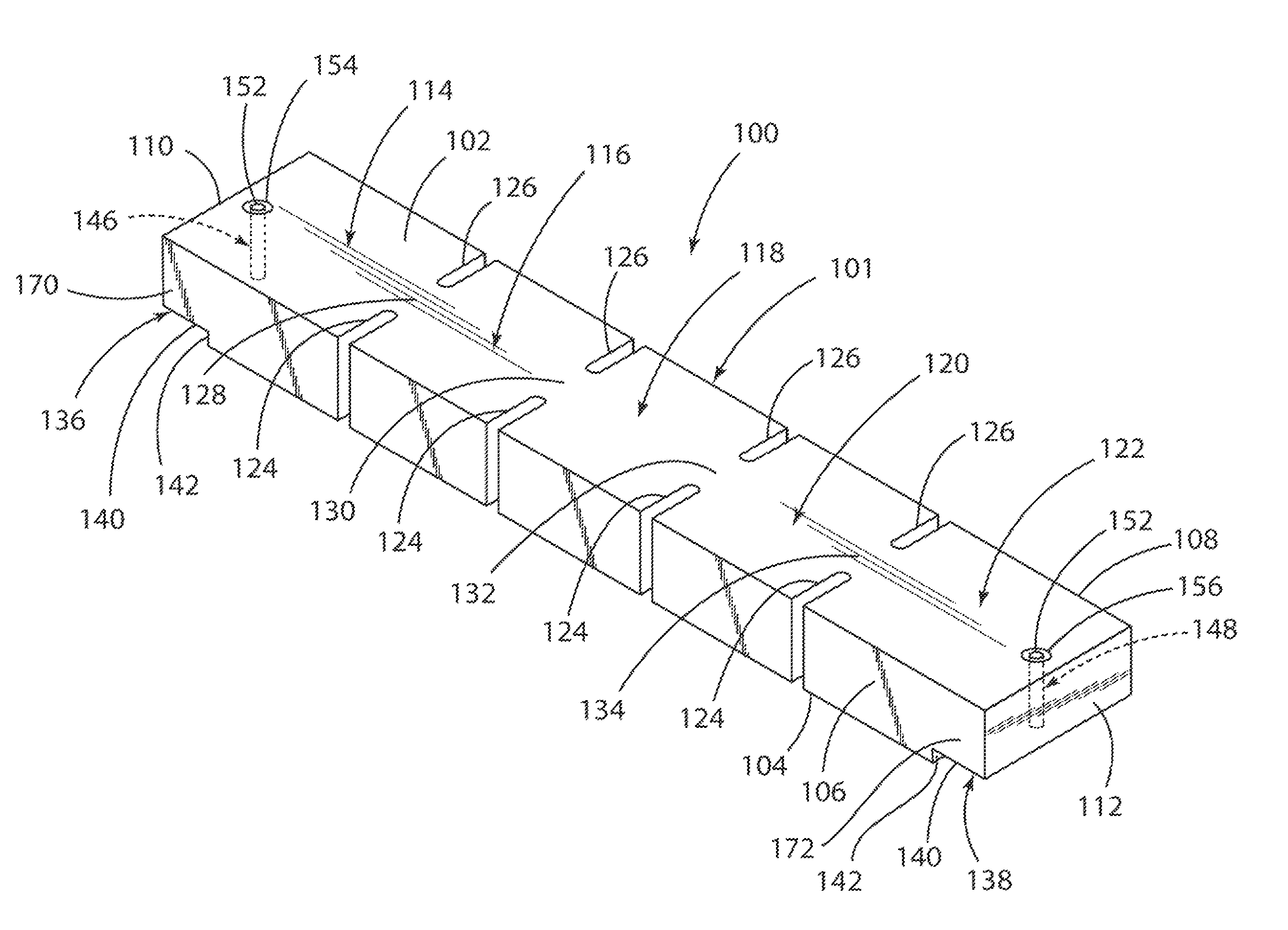
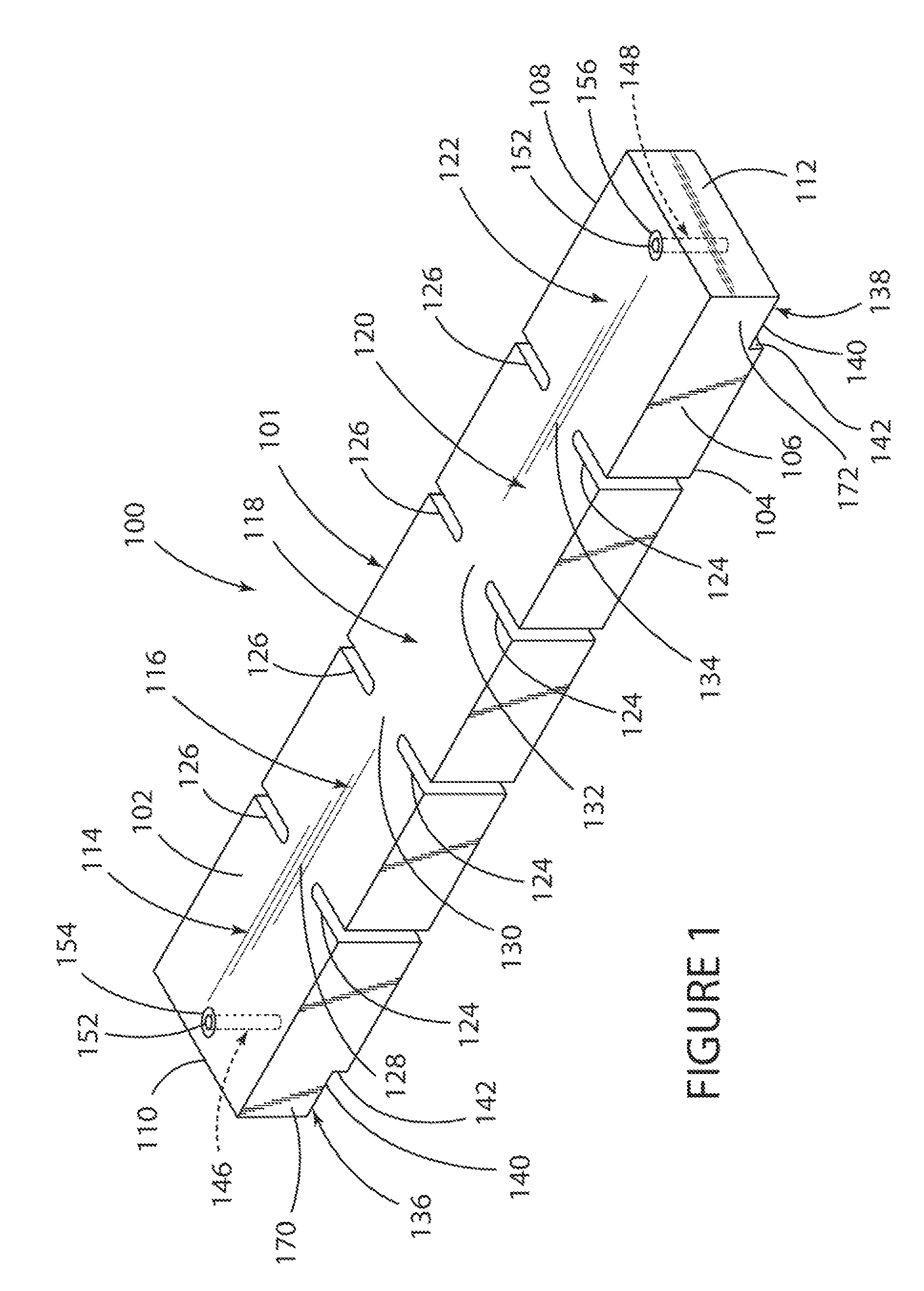
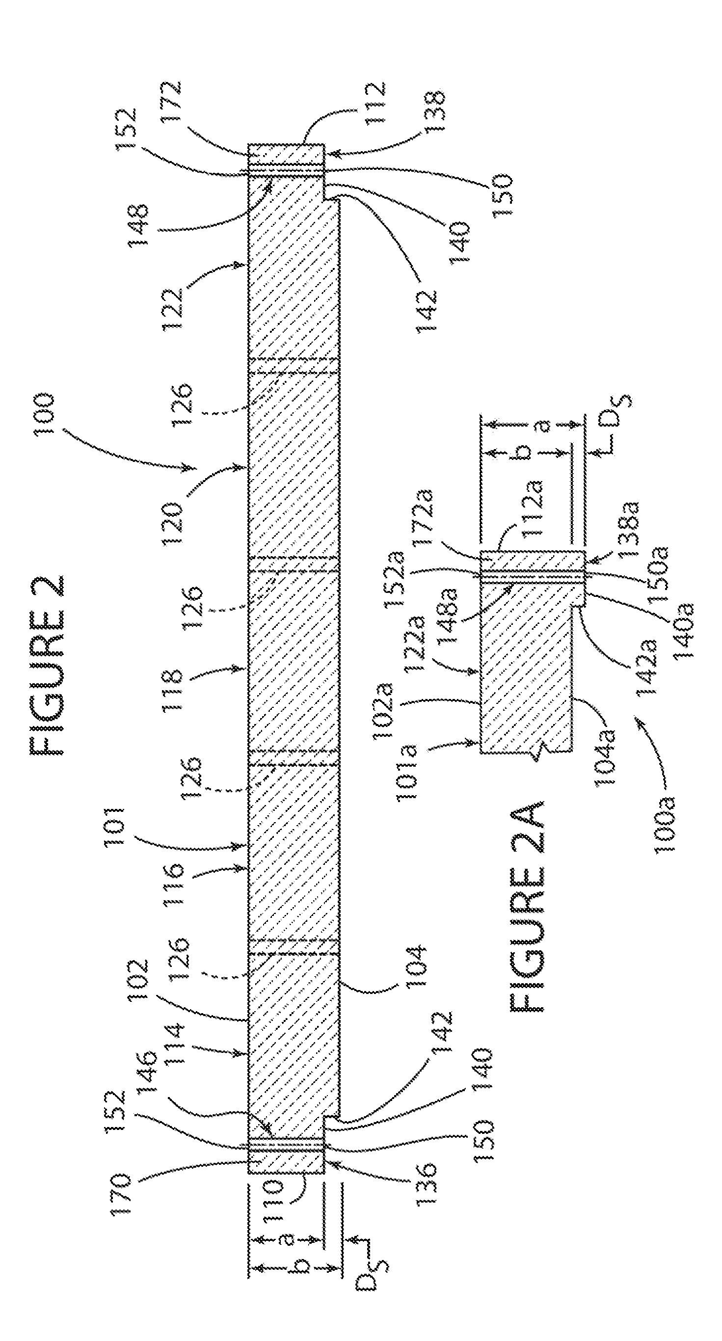
[0035]FIGS. 1 and 2 depict one embodiment of a ceramic dielectric waveguide filter 100 according to the present invention which is made from a generally parallelepiped-shaped monoblock 101, comprised of any suitable dielectric material such as for example ceramic, and having opposed longitudinal upper and lower horizontal exterior surfaces 102 and 104, opposed longitudinal side vertical exterior surfaces 106 and 108, and opposed transverse side vertical exterior end surfaces 110 and 112.

[0036]The monoblock 101 includes a plurality of resonant sections (also referred to as cavities or cells or resonators) 114, 116, 118, 120, and 122 which are spaced longitudinally along the length of the monoblock 101 and are separated from each other by a plurality of spaced-apart vertical slits or slots 124 and 126 which are cut into the surfaces 102, 104, 106, and 108 of the monoblock 101.

[0037]The slits 124 extend along the length of the side surface 106 of the monoblock 101 in a spaced-apart and...


PUM

PropertyMeasurementUnit
heightaaaaaaaaaa
widthaaaaaaaaaa
lengthaaaaaaaaaa

Abstract

A structure and method for adjusting the bandwidth of a ceramic waveguide filter comprising, in one embodiment, a monoblock of dielectric ceramic material defining respective steps and respective input / output through-holes extending through the monoblock and the respective steps. In one embodiment, the steps are defined by notches in the monoblock and the input / output through-holes define openings terminating in the notch. The bandwidth of the ceramic waveguide filter may be adjusted by adjusting the height / thickness and direction of the steps relative to an exterior surface of the monoblock and / or the diameter of the input / output through-holes.

Description

CROSS-REFERENCE TO RELATED APPLICATION[0001]This application claims the benefit of the filing date of U.S. Provisional Patent Application Ser. No. 61 / 345,382 filed on May 17, 2010 and entitled, “Dielectric Waveguide Filter with Structure and Method for Adjusting Bandwidth”, the entire disclosure of which is explicitly incorporated herein by reference as are all references cited therein.FIELD OF THE INVENTION[0002]The invention relates generally to dielectric waveguide filters and, more specifically, to a structure and method for adjusting the bandwidth of a dielectric waveguide filter.BACKGROUND OF THE INVENTION[0003]Ceramic dielectric waveguide filters are well known in the art. In the electronics industry today, ceramic dielectric waveguide filters are typically designed using an “all pole” configuration in which all resonators are tuned to the passband frequencies. With this type of design, one way to increase the attenuation outside of the passband is to increase the number of r...

Claims


Application Information

Patent Timeline
Patent Type & Authority Patents(United States)
IPC IPC(8): H01P1/208
CPCH01P1/2088H01P1/2002H01P7/10H01P11/008Y10T29/49718H01P1/20H01P1/2056H01P1/207
Inventor VANGALA, REDDY
Owner CTS CORP ELKHART
Why Eureka
Try Eureka