An optical waveguide, method for preparing same and wavelength converter

A technology of optical waveguide and waveguide layer, which is applied in the field of communication, can solve the problems of reducing conversion efficiency, low waveguide manufacturing temperature, and enhancement of frequency-doubled optical absorption, so as to reduce photoinduced absorption, widen pump bandwidth, and improve conversion efficiency. Effect

Inactive Publication Date: 2010-03-03
HUAWEI TECH CO LTD +1
View PDF0 Cites 31 Cited by
  • Summary
  • Abstract
  • Description
  • Claims
  • Application Information

AI Technical Summary

Problems solved by technology

[0003] So far, the preparation of LiNbO 3 (Lithium niobate) optical waveguide technologies mainly include Ti diffusion method, annealing proton exchange method (APE) and liquid phase epitaxy film method (LPE), but these three preparation processes are very important for realizing anti-photorefractive effect and reducing polarization dependence. As well as high conversion efficiency PPLN optical waveguides, there are still some defects
For the Ti diffusion method to prepare LiNbO 3 As far as optical waveguides are concerned, although low-loss optical waveguides can be obtained, their wavelength conversion efficiency is low due to the weak optical field confinement and the photorefractive effect in the visible range.
Compared with the Ti diffusion method, the optical waveguide prepared by the APE method has the advantages of low waveguide fabrication temperature, fast waveguide formation, and at least four orders of magnitude stronger resistance to photorefraction than the Ti diffusion waveguide, but it also has some disadvantages: first, use the APE method Prepared LiNbO 3 Optical waveguide, the weak photorefractive effect will still cause the deviation of the quasi-phase matching condition, even if Mg or Zn doped LiNbO 3 Optical waveguide still needs a high operating temperature to suppress the photorefractive effect; secondly, due to the movement of protons in the waveguide, doped LiNbO must be used at low temperature 3 The substrate of the crystal, when the operating temperature rises, allows protons to diffuse into the substrate; finally, the electro-optic effect and second-order nonlinear effect of the optical waveguide after annealing the proton exchange are the same as those of the bulk LiNbO 3 Crystal is much lower than that, and for Z-cut LiNbO 3 As far as the crystal is concerned, the optical waveguide prepared by the APE method only increases the refractive index of the extraordinary light, while the refractive index of the ordinary light decreases slightly. Therefore, the Z-cut optical waveguide prepared by the APE method can only transmit TM mode light, that is, The optical waveguide prepared by APE method itself is a polarization-dependent waveguide
The optical waveguide prepared by the LPE method can increase the refractive index of extraordinary light and ordinary light at the same time, that is, the TE mode and TM mode can exist at the same time, but it also has some problems: first, it is very difficult to grow a thin film with a thickness of more than 5um to make the waveguide layer , and due to the growth rate and defects in the film growth process, the quality of the grown film will be poor, and the coupling efficiency of the optical waveguide and the optical fiber made of the film with a thickness less than 5um is low
[0006] In the process of implementing the present invention, the inventors have found that there are at least the following problems in the prior art: the LiNbO prepared by the prior art scheme 3 The pumping response bandwidth of the optical waveguide is narrow, only 0.15nm, which cannot realize the tunability of the pump light; Under the irradiation of high-intensity laser, the zinc-doped lithium niobate crystal will turn dark brown where the light passes through, forming a wide absorption band covering the visible light region, which leads to the enhanced absorption of frequency-doubled light by the crystal during the frequency-doubling effect, which is extremely Greatly reduces the conversion efficiency

Method used


Image

  • An optical waveguide, method for preparing same and wavelength converter
  • An optical waveguide, method for preparing same and wavelength converter
  • An optical waveguide, method for preparing same and wavelength converter

Examples


Embodiment Construction

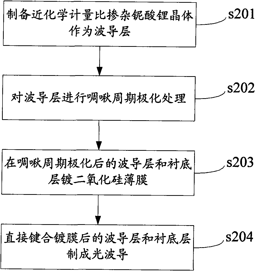
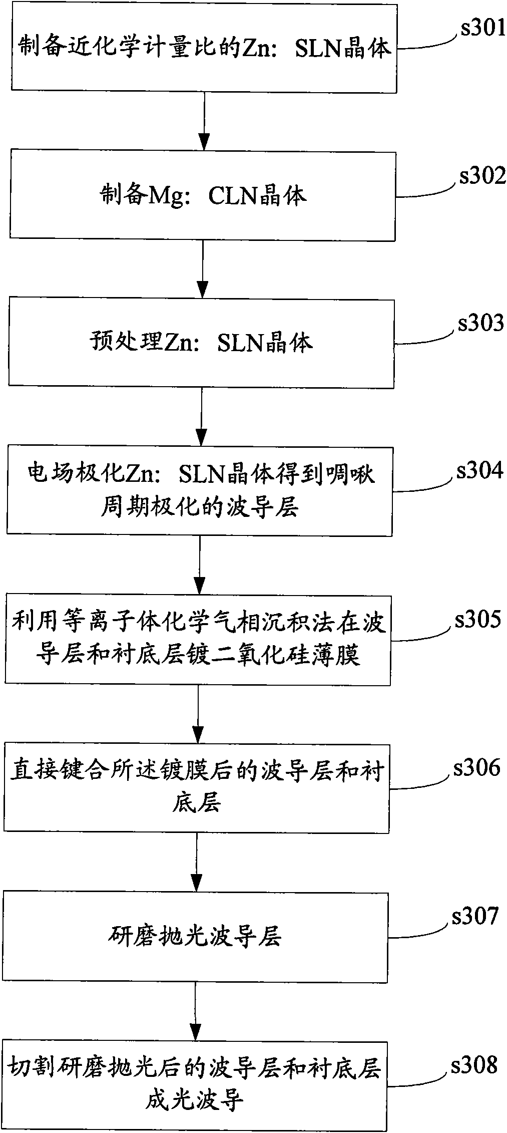
[0025] The present invention will be described below in conjunction with the accompanying drawings and embodiments.

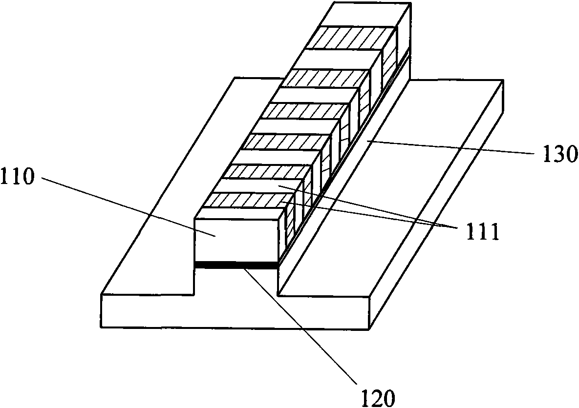
[0026] An embodiment of the present invention provides an optical waveguide, such as figure 1 As shown, the optical waveguide includes a chirped periodically polarized near-stoichiometric lithium niobate crystal waveguide layer 110, a Si-containing film 120 and a substrate 130; the cross-section of the optical waveguide is "convex" Shape: near-stoichiometric doped lithium niobate crystal waveguide layer 110 is on the upper layer of the optical waveguide, and is bonded to the lower substrate 130 through the middle thin film 120 .

[0027] The crystal polarity of the nearly stoichiometric doped lithium niobate crystal waveguide layer 110 changes periodically, and the polarization period increases linearly, forming a chirped periodic grating structure 111; the cross section of the waveguide layer 110 is rectangular or square. The material of the thin film 120 inc...


PUM

PropertyMeasurementUnit
thicknessaaaaaaaaaa

Abstract

The invention discloses an optical waveguide, a method for preparing the same and a wavelength converter. The cross section of the optical waveguide is in a shape like a Chinese character 'tu'; a waveguide layer of a near-stoichiometric doped lithium niobate crystal with a poled chirp period is positioned on the upper layer of the optical waveguide, and is bonded with a lower substrate by a film of which the middle contains Si components. The embodiment of the invention improves the refractivity difference between the substrate and the waveguide layer, restrains the transmission of an opticalsignal in the optical waveguide and improves the conversion efficiency through film coating, widens pump bandwidth through the grating structure with the poled chirp period, reduces the photoinduced absorption effect under the irradiation of high-strong lasers and improves the conversion efficiency by adopting the waveguide layer of the near-stoichiometric doped lithium niobate crystal.

Description

technical field [0001] The invention relates to the communication field, in particular to an optical waveguide, a preparation method thereof and a wavelength converter. Background technique [0002] In Dense Wavelength-Division Multiplexing (DWDM, Dense Wavelength-Division Multiplexing) wavelength routing network, all-optical wavelength conversion technology can realize wavelength reuse, reduce network blocking rate, decentralize network management, and improve network flexibility and reliability. performance and scalability. All-optical wavelength conversion has become the key basic function of wavelength routing, signal regeneration and signal processing in the next generation of high-speed and large-capacity optical communication networks, and has extremely broad application prospects. Currently commonly used all-optical wavelength conversion technologies mainly include: cross-gain modulation (XGM), cross-phase modulation (XPM), nonlinear optical ring cavity (NOLM), lase...

Claims


Application Information

Patent Timeline
Patent Type & Authority Applications(China)
IPC IPC(8): G02B6/10G02B6/13G02F1/37G02F1/35
Inventor 操时宜孙军强周钰杰
Owner HUAWEI TECH CO LTD
Why Eureka
Try Eureka