Nitride semiconductor template and light-emitting diode

a semiconductor and template technology, applied in semiconductor/solid-state device manufacturing, semiconductor devices, electrical devices, etc., can solve the problems of reducing reliability, reducing reliability, and reducing brightness of light-emitting diodes, and achieves low resistance, good crystalline characteristics, and low resistance.

Active Publication Date: 2014-09-09
SUMITOMO CHEM CO LTD
View PDF17 Cites 2 Cited by
  • Summary
  • Abstract
  • Description
  • Claims
  • Application Information

AI Technical Summary

Benefits of technology

[0045]According to one embodiment of the invention, where a substrate (PSS substrate) with convex portions formed on a surface thereof is used as a substrate, it is possible to provide a nitride semiconductor template having low resistance (surface resistivity of not more than 30 Ω / sq) and good crystalline characteristics (XRD half-value width of not less than 50 seconds and not more than 100 seconds), and a light-emitting diode using thereof. In addition, in case of using a planar substrate not having convex portions on a surface thereof (a substrate other than the PSS substrate), it is possible to provide a nitride semiconductor template having low resistance (surface resistivity of not more than 30 Ω / sq) and good crystalline characteristics (XRD half-value width of not less than 50 seconds and not more than 300 seconds), and a light-emitting diode using thereof.

Problems solved by technology

However, increasing the amount of impurity added to the uppermost layer deteriorates crystalline characteristics, which results in a decrease in brightness of the light-emitting diode.
In addition, when the impurity amount is large, brightness is reduced due to dopant diffusion into a light-emitting portion, especially into an active layer, formed on the template and reliability decreases due to the dopant diffusion.
If the impurity is increased to increase the carrier concentration, the impurity in the nitride semiconductor template is diffused into the light-emitting layer during growth of the light-emitting layer portion by the MOVPE method performed later on, which decreases reliability as LED.

Method used


Image

  • Nitride semiconductor template and light-emitting diode
  • Nitride semiconductor template and light-emitting diode
  • Nitride semiconductor template and light-emitting diode

Examples


example 1

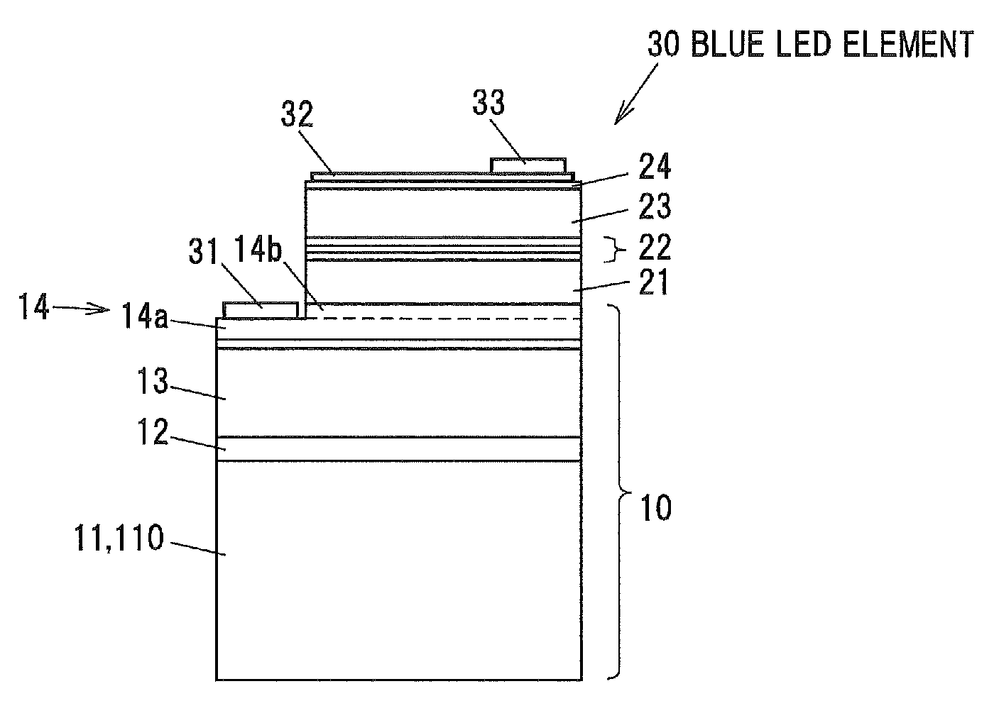
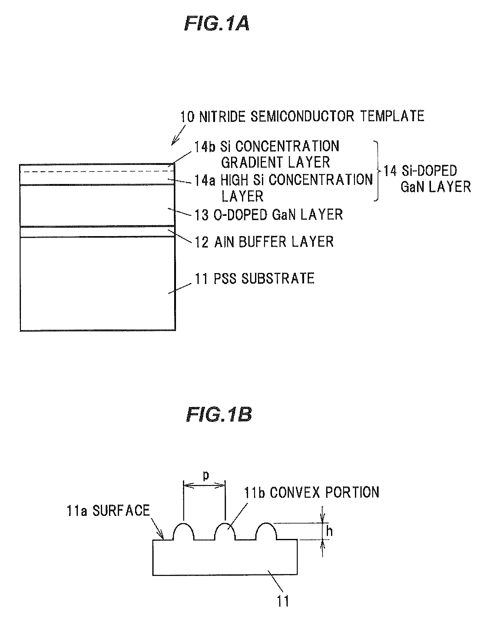
[0106]FIG. 5 is a schematic view showing a structural example of an HVPE apparatus in Examples of the invention. In Example 1, 20 nm of the AlN buffer layer 12 was grown on the PSS substrate 11 using an HVPE apparatus 1 shown in FIG. 5, 6 μm of the O-doped GaN layer 13 was subsequently grown after the growth of the AlN buffer layer 12, and 2 μm of the Si-doped GaN layer 14 was further grown thereon. 0.5 μm of the outermost layer of the Si-doped GaN layer 14 was grown while changing the additive amount of Si. The layer formed while gradually reducing the additive amount of Si is the Si concentration gradient layer 14b. The HVPE apparatus 1 is divided into a raw material portion 3a located at upstream and a growth portion 3b located at downstream, which are respectively heated to about 850° C. and 1100° C. respectively by a raw material portion heater 4a and a growth portion heater 4b.

[0107]Four gas supply lines 6, which are a doping line 61, a group V line 62, a group III (Ga) line ...

example 2

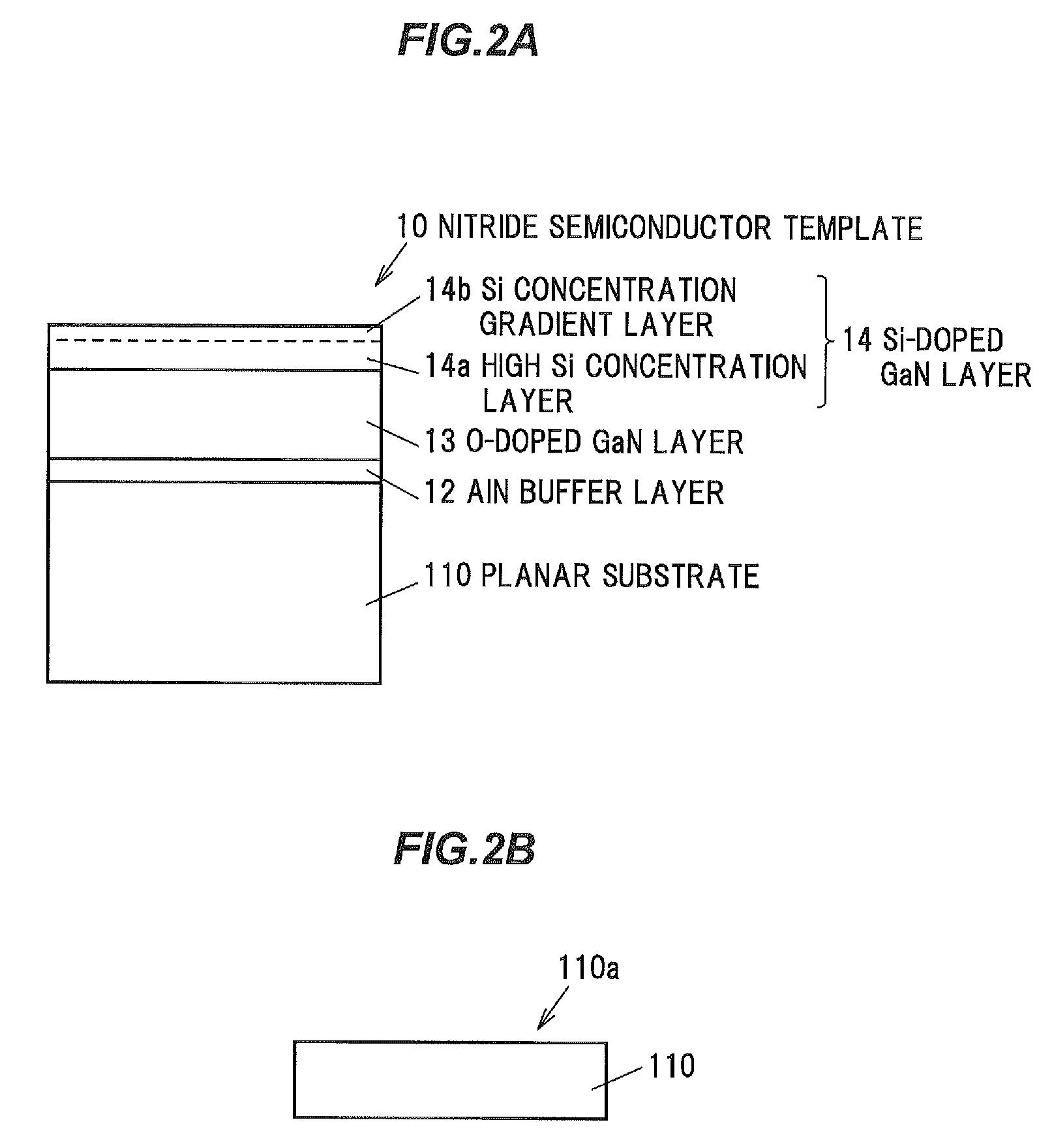
[0133]In Example 2, the nitride semiconductor template 10 was made under the same basal conditions as Example 1. However, some features in Example 2 are different from Example 1. Accordingly, only the difference from Example 1 will be described blow.

[0134]In Example 1, the O-doped GaN layer 13 was grown for growth time of 10 minutes so as to have a thickness of about 6 μm. Meanwhile, in Example 2, the O-doped GaN layer 13 was grown for growth time of 13 minutes so as to have a film thickness of about 8 μm. Accordingly, the total film thickness of the epitaxial layer was about 10 μm.

[0135]In addition, the gas supplied through the group III (Ga) line 63 was a mixture of 50 sccm of HCl gas, 450 sccm of hydrogen and 2000 sccm of nitrogen in Example 1 but was a mixture of 2000 sccm of hydrogen and 450 sccm of nitrogen in Example 2.

[0136]The nitride semiconductor template 10 in Example 2 had a narrow XRD half-value width of 50.1 seconds and surface resistivity of 11 Ω / sq, hence, a better ...

example 3

[0138]In Example 3, the nitride semiconductor template 10 was made under substantially the same conditions as those in Example 1 so that the carrier concentration on the outermost surface of the Si concentration gradient layer 14b is 5×1017 cm−3. The nitride semiconductor template 10 in Example 3 had a narrow XRD half-value width of 74.5 seconds and surface resistivity of 15 Ω / sq. The 34 mW of light emission output was achieved and relative output was 99.7%, and therefore, it was confirmed that the blue LED element 30 has sufficient reliability characteristics.


PUM

PropertyMeasurementUnit
thicknessaaaaaaaaaa
thicknessaaaaaaaaaa
carrier concentrationaaaaaaaaaa

Abstract

A nitride semiconductor template includes a substrate, and a group III nitride semiconductor layer formed on the substrate and including a Si-doped layer doped with Si as an uppermost layer thereof. The group III nitride semiconductor layer has a total thickness of not less than 4 μm and not more than 10 μm. The Si-doped layer includes a Si concentration gradient layer having a carrier concentration that gradually decreases toward an outermost surface thereof so as to be not less than 1×1017 cm−3 and not more than 5×1017 cm−3 at the outermost surface of the group III nitride semiconductor layer.

Description

[0001]The present application is based on Japanese patent application Nos. 2011-274222 and 2012-250072 filed on Dec. 15, 2011 and Nov. 14, 2012, respectively, the entire contents of which are incorporated herein by reference.BACKGROUND OF THE INVENTION[0002]1. Field of the Invention[0003]The invention relates to a nitride semiconductor template and a light-emitting diode using the nitride semiconductor template.[0004]2. Description of the Related Art[0005]Nitride-based compound semiconductors such as gallium nitride (GaN), aluminum gallium nitride (AlGaN) and indium gallium nitride (InGaN) have received attention as a light-emitting element material capable of emitting light from red to ultraviolet. One of crystal growth methods of such nitride semiconductor materials is a Hydride Vapor Phase Epitaxy (HVPE) method in which metal chloride gas and ammonia are used as raw materials.[0006]The HVPE method is characterized in that it is possible to obtain a growth rate of not less than 10...

Claims


Application Information

Patent Timeline
Patent Type & Authority Patents(United States)
IPC IPC(8): H01L33/06H01L29/36H01L33/02H01L33/32
CPCH01L29/36H01L33/025H01L33/325H01L33/06H01L21/0242H01L21/0243H01L21/02458H01L21/02502H01L21/0254H01L21/02573H01L21/02576H01L21/0262
Inventor KONNO, TAICHIROOFUJIKURA, HAJIME
Owner SUMITOMO CHEM CO LTD
Why Eureka
Try Eureka