Semiconductor memory device having three-dimensionally arranged memory cells, and manufacturing method thereof

a memory cell and semiconductor technology, applied in the direction of semiconductor devices, electrical devices, transistors, etc., can solve the problem of difficult to form perfectly perpendicular memory holes in the memory hole formation process, and achieve the effect of increasing the efficiency of the hole passag

Active Publication Date: 2014-09-09
KIOXIA CORP
View PDF4 Cites 20 Cited by
  • Summary
  • Abstract
  • Description
  • Claims
  • Application Information

AI Technical Summary

Problems solved by technology

However, it is difficult to form a perfectly perpendicular memory hole in this memory hole formation process.

Method used


Image

  • Semiconductor memory device having three-dimensionally arranged memory cells, and manufacturing method thereof
  • Semiconductor memory device having three-dimensionally arranged memory cells, and manufacturing method thereof
  • Semiconductor memory device having three-dimensionally arranged memory cells, and manufacturing method thereof

Examples


first embodiment

[2] First Embodiment

[0033]In a first embodiment, the trap density of a charge storage layer is varied between the upper side and lower side in the MONOS structure of a memory cell transistor MTr in a NAND string 10, thereby improving memory cell characteristics.

[0034][2-1] Structure of NAND String

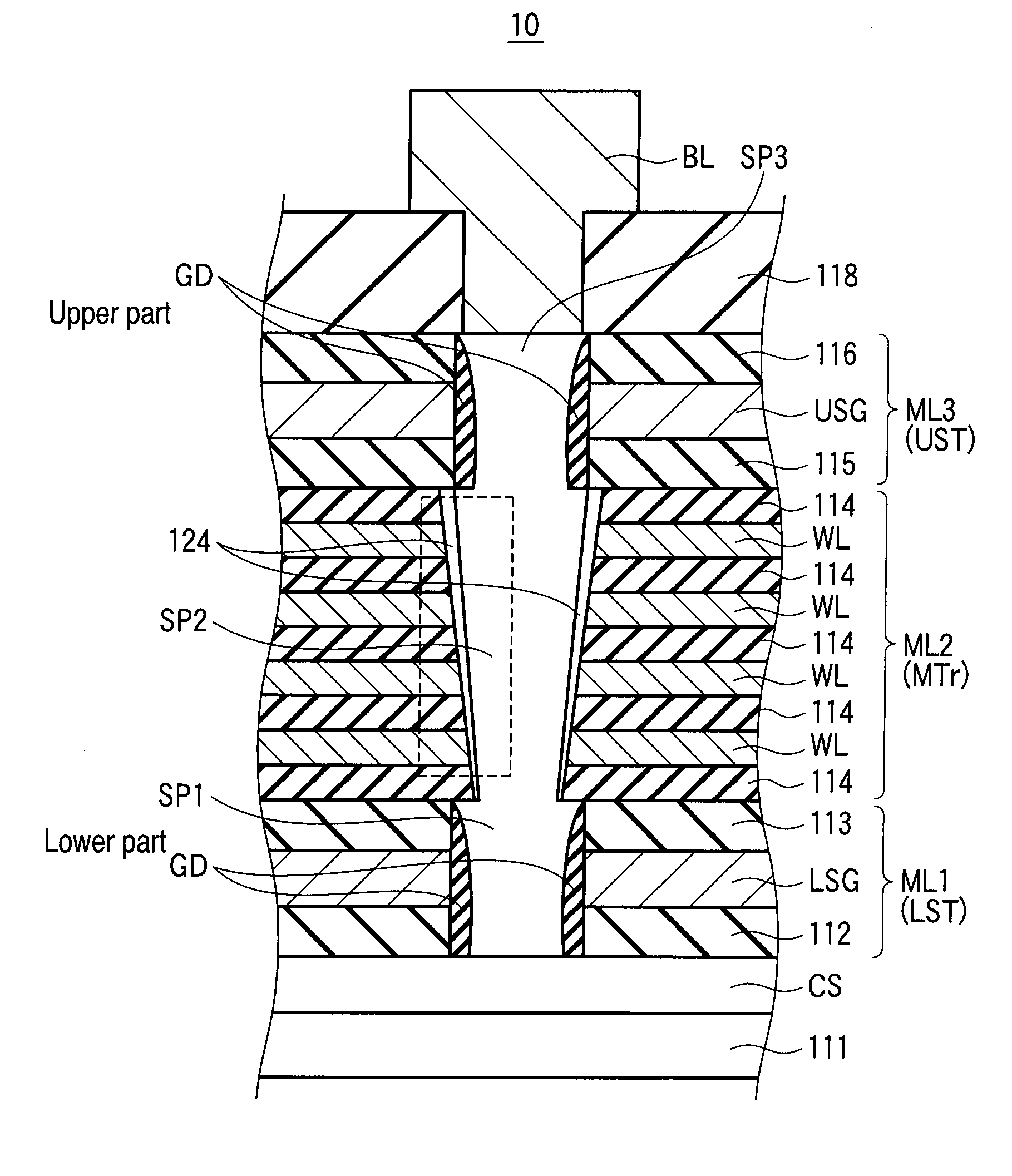
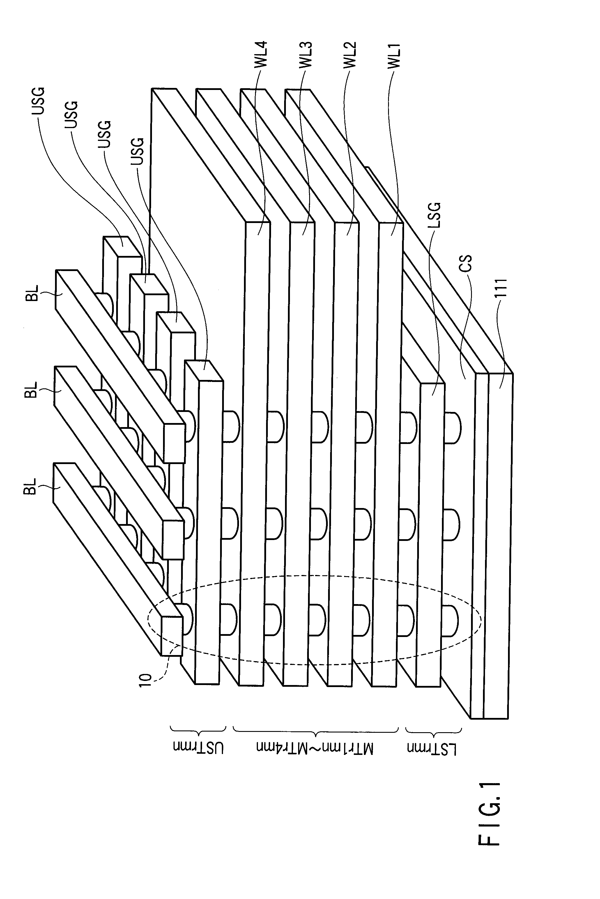
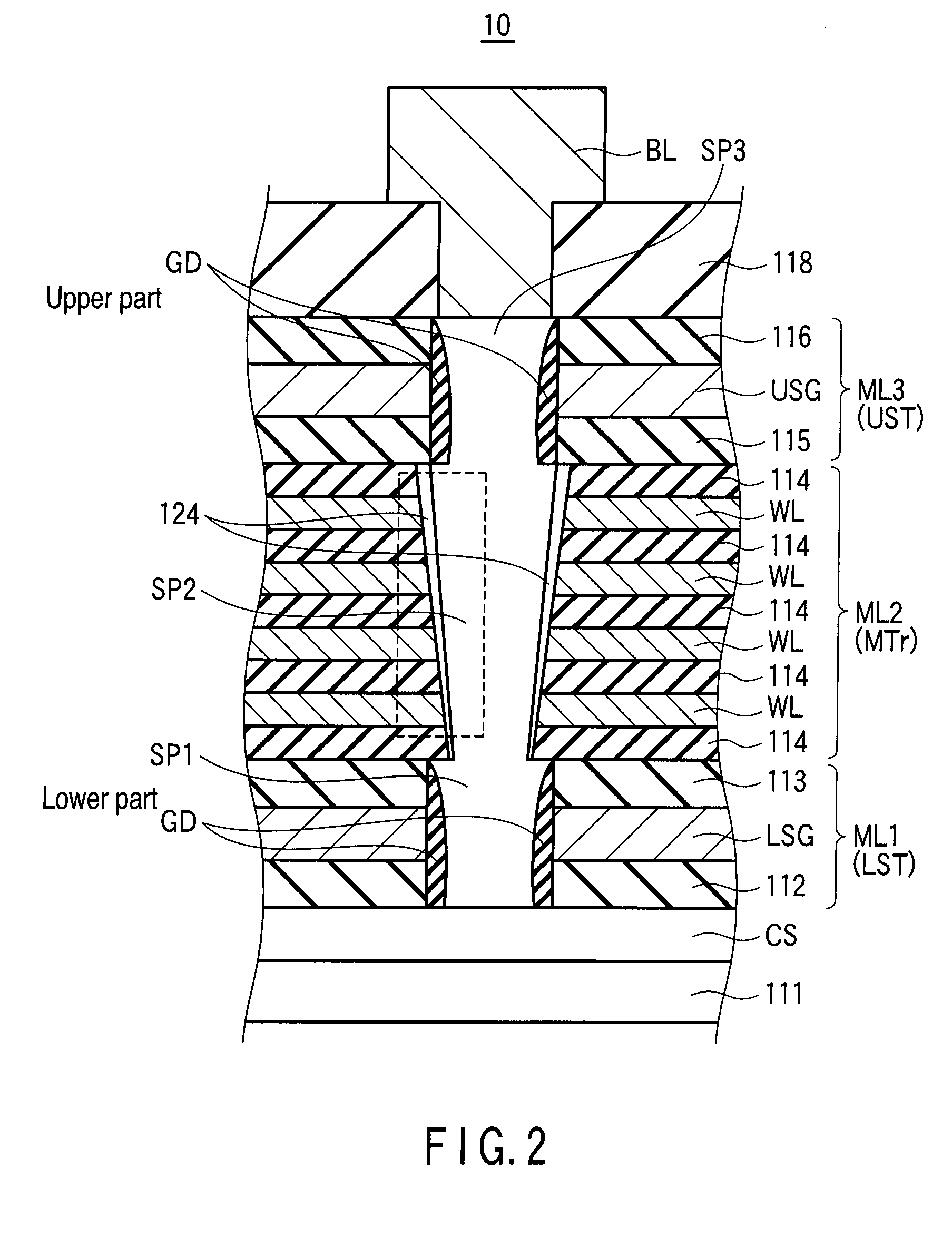
[0035]FIG. 2 shows the configuration of the NAND string 10 according to the first embodiment.

[0036]As shown in FIG. 2, the NAND string 10 comprises a semiconductor substrate (silicon substrate) 111, a low-resistance layer CS, a lower select transistor LST, the memory cell transistor MTr, an upper select transistor UST, an element isolation dielectric film 118 and a bit line BL.

[0037]The impurity-introduced low-resistance layer CS (e.g., an n+ diffusion layer) serving as a source line is formed on the semiconductor substrate 111. A silicon pillar (semiconductor pillar) SP1 is formed on the low-resistance layer CS perpendicularly to the surface of the semiconductor substrate 111. A gate diele...

second embodiment

[3] Second Embodiment

[0097]In the first embodiment, the trap density of the charge storage layer is varied between the upper and lower sides in the MONOS structure of the memory cell transistor. On the contrary, in the second embodiment, the hole passage efficiency of the tunnel dielectric film is varied between the upper and lower sides in the MONOS structure to improve memory cell characteristics. It is to be noted that similarities between the second embodiment and the first embodiment are not described and differences are described in detail.

[0098][3-1] Structure of NAND string

[0099]FIG. 14 shows the configuration of a NAND string 10 according to the second embodiment.

[0100]As shown in FIG. 14, the difference between the NAND string 10 in the present embodiment and the NAND string 10 in the first embodiment is in the configuration of a memory film 224.

[0101]FIG. 15A shows the configuration of the memory film 224 of a memory cell transistor MTr according to the present embodiment...


PUM


Abstract

A first select transistor is formed on a semiconductor substrate. Memory cell transistors are stacked on the first select transistor and connected in series. A second select transistor is formed on the memory cell transistors. The memory cell transistors include a tapered semiconductor pillar which increases in diameter from the first select transistor toward the second select transistor, a tunnel dielectric film formed on the side surface of the semiconductor pillar, a charge storage layer which is formed on the side surface of the tunnel dielectric film and which increases in charge trap density from the first select transistor side toward the second select transistor side, a block dielectric film formed on the side surface of the charge storage layer, and conductor films which are formed on the side surface of the block dielectric film and which serve as gate electrodes.

Description

CROSS-REFERENCE TO RELATED APPLICATIONS[0001]This application is based upon and claims the benefit of priority from prior Japanese Patent Application No. 2009-068963, filed Mar. 19, 2009, the entire contents of which are incorporated herein by reference.BACKGROUND OF THE INVENTION[0002]1. Field of the Invention[0003]The present invention relates to a semiconductor memory device having memory cell transistors perpendicularly stacked on a substrate, and a manufacturing method thereof.[0004]2. Description of the Related Art[0005]In connection with NAND-type flash memories, there has been developed, for example, a three-dimensional stack memory wherein memory cells and select transistors constituting a memory string (NAND string) are stacked. There has also been developed a technique for collectively forming the memory cells and select transistors (e.g., see Jpn. Pat. Appln. KOKAI Publication No. 2007-266143). According to this technique, element isolation dielectric films and electrode...

Claims


Application Information

Patent Timeline
Patent Type & Authority Patents(United States)
IPC IPC(8): H01L29/792H01L21/336H01L27/115H01L29/423H01L29/788
CPCH01L27/11578H01L29/42332H01L27/11582H01L29/7881H01L27/11551H01L27/11556H01L29/792H01L29/7926H10B41/20H10B43/20H10B41/27H10B43/27
Inventor SEKINE, KATSUYUKITAKANO, KENSUKEHIGUCHI, MASAAKIKAI, TETSUYAOZAWA, YOSHIO
Owner KIOXIA CORP
Why Eureka
Try Eureka