Touch screen panel active matrix organic light emitting diode display device

a technology of organic light-emitting diodes and display devices, which is applied in the field of display devices to achieve the effect of preventing damage to amoled and reducing the thickness of the amoled display devices

Active Publication Date: 2014-09-09
SAMSUNG ELECTRONICS CO LTD
View PDF7 Cites 20 Cited by
  • Summary
  • Abstract
  • Description
  • Claims
  • Application Information

AI Technical Summary

Benefits of technology

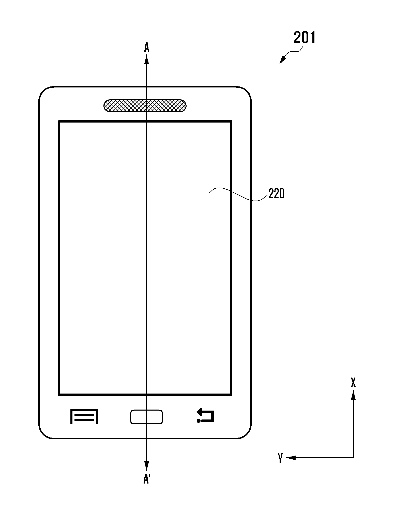
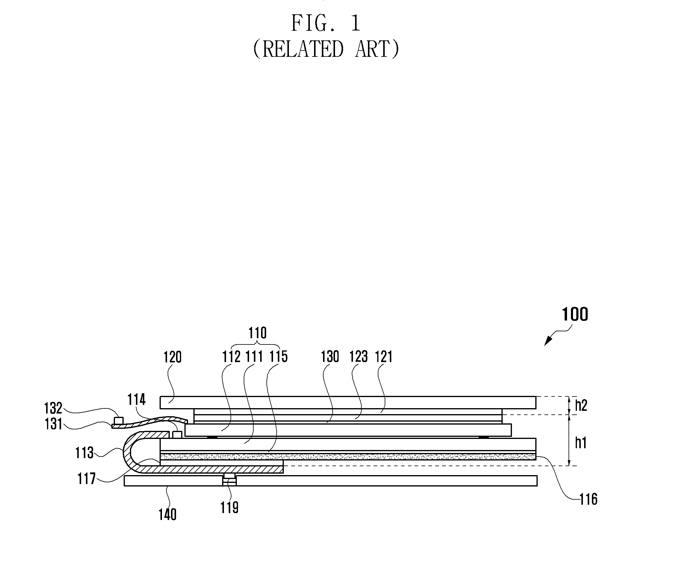
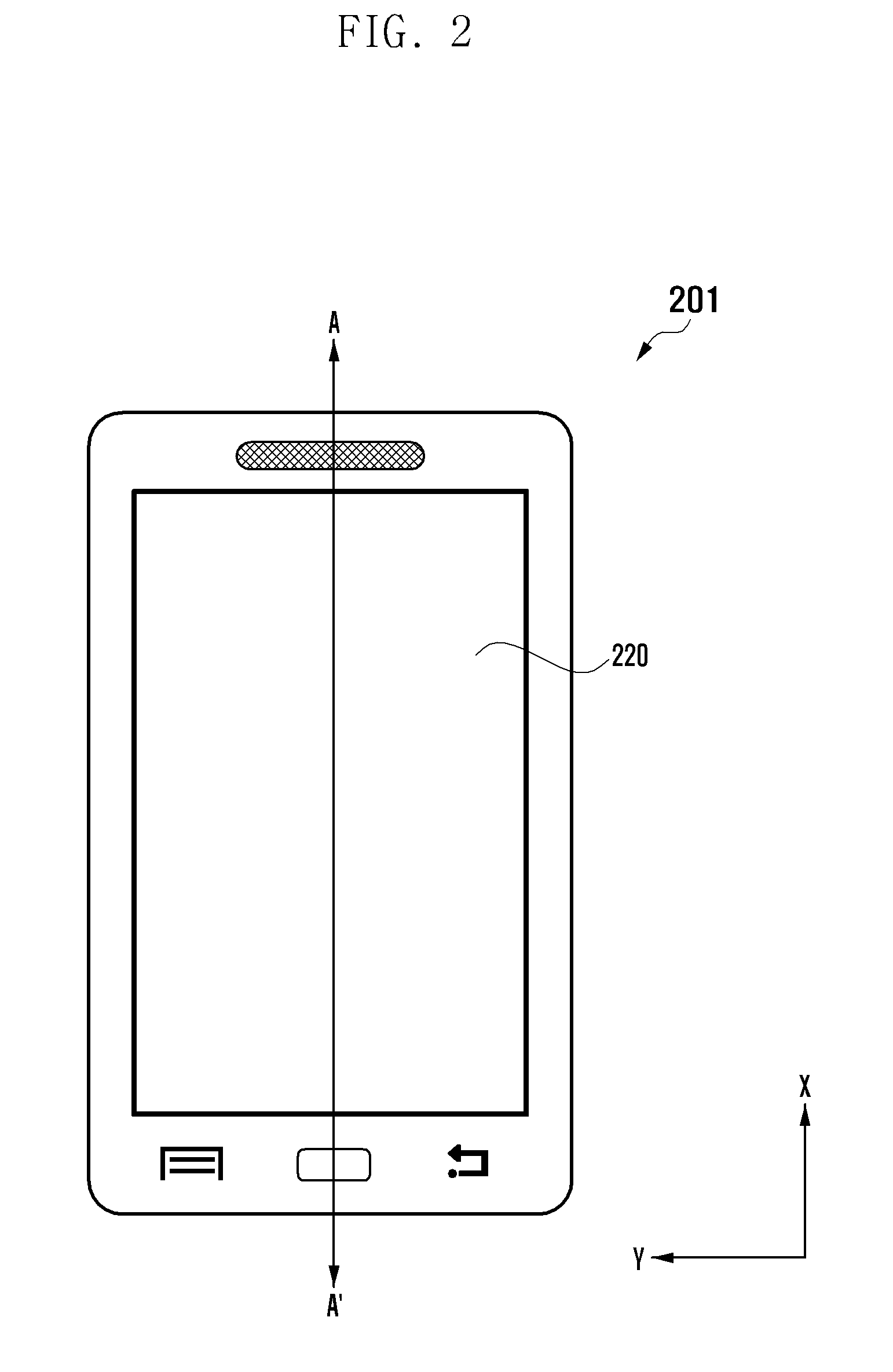
[0010]Aspects of the present invention are to address the above mentioned problems and / or disadvantages and to provide at least the advantages described below. Accordingly, an aspect of the present invention is to provide a touch screen panel Active Matrix Organic Light Emitting Diode (AMOLED) display device to decrease the thickness of the touch screen panel AMOLED display device, and prevent damage to the AMOLED due to an external shock.
[0011]Another aspect of the present invention is to provide a touch screen panel AMOLED display device that prevents separation of a flexible AMOLED driver Integrated Circuit (IC) from a mounting surface and damage thereof.
[0013]According to exemplary embodiments of the present invention, the thickness of the touch screen panel AMOLED display device may be decreased and damage to the AMOLED due to external shock may be prevented by using the flexible AMOLED. Additionally, separation of the flexible AMOLED driver IC from the mounting surface may be prevented by using a COF film on which the flexible AMOLED driver IC is mounted.
[0014]Additionally, damage to the flexible AMOLED driver IC due to external shock may be prevented by attaching a buffer member that protects the flexible AMOLED driver IC from external shock to the rear of the flexible AMOLED.

Problems solved by technology

Also, there are problems in that the AMOLED 110 may be damaged due to an external shock and that the AMOLED driver IC 114 mounted on the LTPS glass 111 may be separated from the LTPS glass 111.

Method used


Image

  • Touch screen panel active matrix organic light emitting diode display device
  • Touch screen panel active matrix organic light emitting diode display device
  • Touch screen panel active matrix organic light emitting diode display device

Examples


Embodiment Construction

[0022]The following description with reference to the accompanying drawings is provided to assist in a comprehensive understanding of exemplary embodiments of the invention as defined by the claims and their equivalents. It includes various specific details to assist in that understanding but these are to be regarded as merely exemplary. Accordingly, those of ordinary skill in the art will recognize that various changes and modifications of the embodiments described herein can be made without departing from the scope and spirit of the invention. In addition, descriptions of well-known functions and constructions may be omitted for clarity and conciseness.

[0023]The terms and words used in the following description and claims are not limited to their bibliographical meanings, but, are merely used by the inventor to enable a clear and consistent understanding of the invention. Accordingly, it should be apparent to those skilled in the art that the following description of exemplary emb...


PUM


Abstract

A touch screen panel Active Matrix Organic Light Emitting Diode (AMOLED) display device for decreasing the thickness of a mobile terminal and improving a degree of freedom in design is provided. The touch screen panel AMOLED display device includes a flexible AMOLED disposed on the bottom of a window, and a Chip-On-Film (COF) film connected to the flexible AMOLED and coupled with a flexible AMOLED driver Integrated Circuit (IC). Therefore, the thickness of the touch screen panel AMOLED display device may be decreased, and damage of the AMOLED due to an external shock may be prevented. Additionally, separation of the flexible AMOLED driver IC from a mounting surface may be prevented.

Description

PRIORITY[0001]This application claims the benefit under 35 U.S.C. §119(a) of a Korean patent application filed on Jul. 13, 2011 in the Korean Intellectual Property Office and assigned Serial No. 10-2011-0069261, the entire disclosure of which is hereby incorporated by reference.BACKGROUND OF THE INVENTION[0002]1. Field of the Invention[0003]The present invention relates to a display device including a touch screen panel. More particularly, the present invention relates to a touch screen panel Active Matrix Organic Light Emitting Diode (AMOLED) display device.[0004]2. Description of the Related Art[0005]Recently, touch screen panel display devices have been applied to mobile terminals to decrease the weight and thickness of the mobile terminal and to increase a display area thereof Among various touch screen panel display devices, a touch screen panel AMOLED display device that uses an AMOLED having a high optical characteristic is used most frequently.[0006]FIG. 1 is a cross-section...

Claims


Application Information

Patent Timeline
Patent Type & Authority Patents(United States)
IPC IPC(8): G06F3/041H01L27/32H04M1/02H04M1/18H05K1/14
CPCH01L27/323H04M1/0266H04M1/18H05K1/147G06F3/0412H10K59/40H10K50/805H10K50/816
Inventor EOM, SANG YONGKIM, DONG SUB
Owner SAMSUNG ELECTRONICS CO LTD
Why Eureka
Try Eureka