
Light emitting diode array structure, and printing head and printing device thereof

a technology of light-emitting diodes and arrays, which is applied in the direction of semiconductor devices, printing, electrical devices, etc., can solve the problems of further limited area of leds and limited light emission of leds, and achieve the effect of raising light emission and improving photoconductivity and printing speed of printing devices

Active Publication Date: 2014-09-23
AVISION
View PDF4 Cites 0 Cited by
  • Summary
  • Abstract
  • Description
  • Claims
  • Application Information

AI Technical Summary

Benefits of technology

This configuration increases the light emission amount and improves printing speed by maintaining high arrangement density and distribution area of light emitting thyristors, effectively addressing the limitations of existing LED array structures in achieving higher printing resolutions and speeds.

Problems solved by technology

However, the area of an LED is further limited, and a light emission amount of the LED is limited.

Method used


Image

  • Light emitting diode array structure, and printing head and printing device thereof
  • Light emitting diode array structure, and printing head and printing device thereof
  • Light emitting diode array structure, and printing head and printing device thereof

Examples


Embodiment Construction

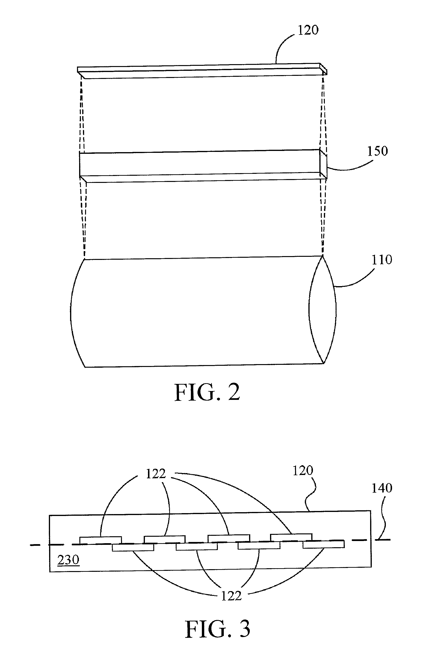
[0026]FIG. 2 is a schematic view of photoconductivity of a printing device according to an embodiment.

[0027]As shown in FIG. 2, the printing device includes a photoconductive drum 110, a printing head 120, and a lens 150. The lens 150 is located between the photoconductive drum 110 and the printing head 120, and is used to focus light emitted by the printing head 120 on the photoconductive drum 110, so as to implement the foregoing exposure procedure.

[0028]The number of the photoconductive drum 110, the printing head 120, and the lens 150 may be one to perform black-and-white printing. However, the embodiments of the disclosure are not limited thereto. The number of the photoconductive drums 110, the printing heads 120, and the lenses 150 may be four respectively to correspond to the purposes of color printing related to black, magenta, cyan, and yellow. The printing device may be a printer, a photocopier, a multifunction peripheral, and the like.

[0029]FIG. 3 is a schematic view of ...


PUM


Abstract

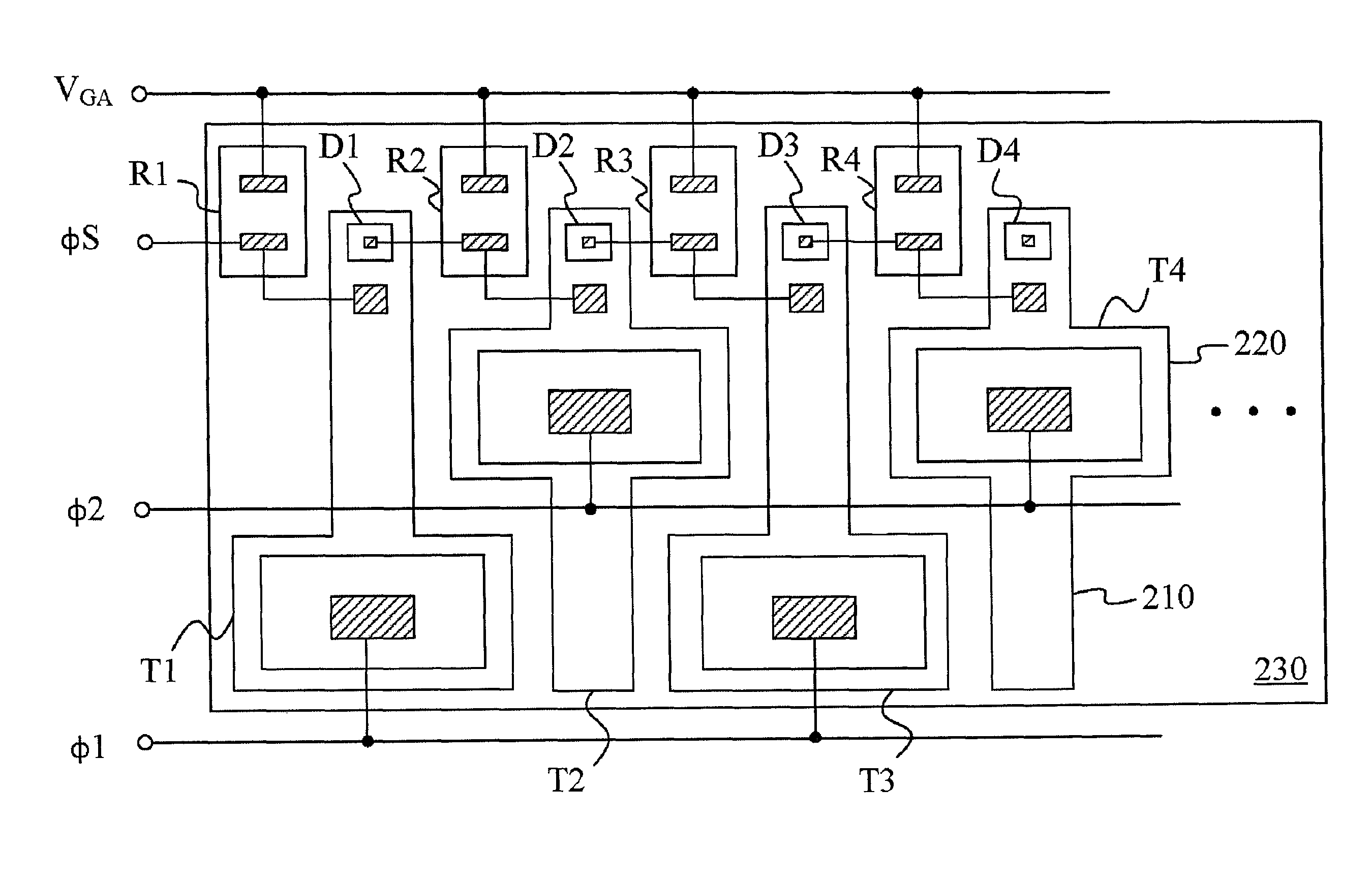
A light emitting diode (LED) array structure includes a substrate and a plurality of light emitting thyristors. The light emitting thyristors are arranged linearly on the substrate. Each light emitting thyristor includes a strip portion and a plate portion connected to each other, and the plate portions of the adjacent light emitting thyristors are staggered with each other, so as to maintain an arrangement density of the light emitting thyristors, and increase a distribution area of the light emitting thyristors. A printing head and a printing device with the foregoing LED array structure are also provided herein, so as to improve photoconductivity and printing speed of the printing device through the light emitting thyristors, which provide a raised light emission amount by increasing the distribution area.

Description

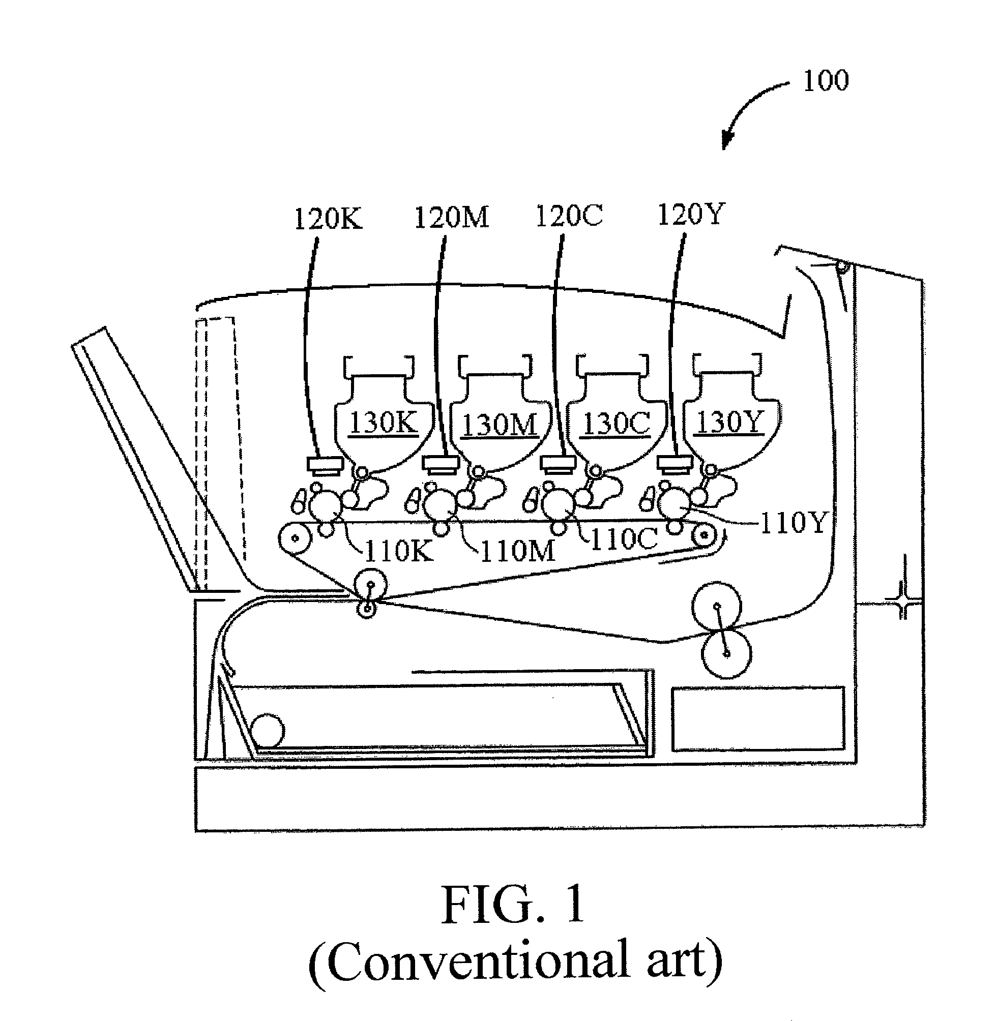
CROSS-REFERENCES TO RELATED APPLICATIONS[0001]This non-provisional application claims priority under 35 U.S.C. §119(a) on Patent Application No. 101140414 filed in Taiwan, R.O.C. on 2012 Oct. 31, the entire contents of which are hereby incorporated by reference.BACKGROUND[0002]1. Technical Field[0003]The disclosure relates to a diode array structure, and more particularly to a light emitting diode (LED) array structure, and a printing head and a printing device thereof.[0004]2. Related Art[0005]A photocopier, a printer, a fax machine, and a multifunction peripheral use electro-photography as a core technology for printing a document; that is, the devices generate a photographic image by changing the distribution of electrostatic charges through light with a specific wavelength.[0006]Please refer to FIG. 1, which is a schematic view of a LED printer 100 for color printing. The LED printer 100 has photoconductive drums (110K, 110M, 110C, and 110Y, referred to in sum as 110), printing ...

Claims


Application Information

Patent Timeline
Patent Type & Authority Patents(United States)
IPC IPC(8): B41J2/45H01L31/12H01L27/15
CPCB41J2/45H01L27/156H01L25/0753H01L33/0004H01L33/20H01L2924/0002H01L2924/00
Inventor CHANG, TZ-LIANGPENG, PO-HSIUNG
Owner AVISION
Learn More